| Advantages |
FOWLP is conventional fan- out
WLP with molding & wafer level
RDL technology
Smaller form-factor, Thinner profile
and substrate-less package
Higher electrical performance with
lower transmission loss of shorter
electrical path
|
With M-Series and Adaptive Patterning®,the barriers to chips-first,
high-density fan-out disappear
Die shift and warpage control through Adaptive patterning 6 sides protection
for Higher board level reliability with M-Series
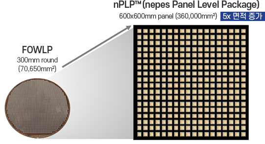
PLP (600mm Panel) is a technology that can utilize the area more efficiently
than the 300mm Round Panel. Fit 5x more 300mm wafers in one panel
through 600mm panel size
|
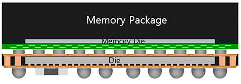
Very thin package profile even package stacking platform of Process
& Memory packages. The smallest Form factor (smaller size & thinner profile)
Highly integration with multi-layer RDLs and finer line & space pitch of
5um. Stackable package through Cu Post vertical interconnection technology
Higher Electrical & Thermal Performance compared to conventional PoP
packages with very shortest electrical path and higher ration of silicon
chip inside bottom package.
|
| Features |
High Reliability
Meets JEDEC MSL3 CLR and BLR
requirements
Slim & Small formfactor
Integration & Size with SiP
|
High Reliability
Meets JEDEC MSL3 CLR and BLR requirements
Slim & Small formfactor
Flexible productivity
Cost effectiveness
|
Attributes: Package & Die Size:
14mmX15mm & 12mmX11mm
IO: ~1500�Backside 2-RDL(8um L/S)
Frontside 3-RDL(5um L/S)
Cu Post 90um CD, 60um Space
|
Package size : 14mm x 15mm
Package thickness : 310um
( 230um w/o BGA )
Chip size : 10.9mm x 11.7mm
Double side RDL : Front-side(4P4M ),
Back-side( 3P3M )
Cu-post pitch : 150um,
Cu-post height : 160±10um
Fine-pitch RDL : L/S=5/5um,
Min. via diameter=Ø15um
Min. chip pad pitch : 90um
|
| Application |
Communication, Consumer, Automotive, Industrial, Computer,
(RF, PMIC, AP, Connectivity, Baseband, Audio codec, sensor, (x)PU) |


