To provide high functional materials
to next generation nano-device
Negative Photoresist

Negative Thick photoresist for Wafer Level Package - RDL, CPB
-
Cu RDL (Redistribution Layer)
- PR pattern
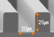
- Cu RDL
-
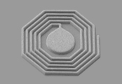
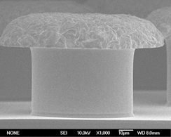
CPB (Cu Pillar Bump)
- PR pattern
- CPB
- Polymer 및 formulation 디자인 기술 확보
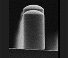
- 우수한 pattern profile (no footing, no under-cut)
- 우수한 공정 마진
- 빠른 공정 속도
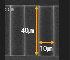
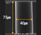
- 높은 해상도 및 종횡비
- 뛰어난 내도금성
Positive Photoresist
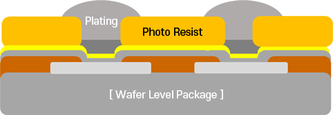
Positive Thick photoresist for TSV, CPB
-
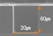
TSV (Trough Silicon Via)
- PR pattern
- Plating
-
CPB (Cu Pillar Bump)
- PR pattern
- Plating
-
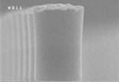
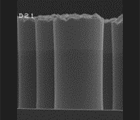
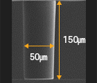
Tall Pillar
- PR pattern
- 자체 폴리머 설계 및 조성 최적화
- 좋은 pattern profile (no footing, no under-cut)
- 뛰어난 스트립성 (PR 잔사 無)
- 고해상력 / 높은 종횡비
- 넓은 공정 마진
- 우수한 내화학성 및 내도금성
Photo-definable Dielectiric
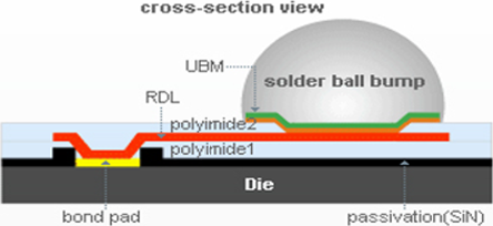
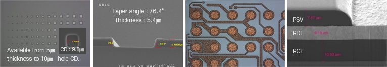
Photo-definable dielectric for advanced package
- NDP-Series는 bumping 공정에서 다양한 보호/ 절연층으로 사용
- Soluble Polyimide backbone : 초저온 경화, 초저수축율 구현
PR Stripper
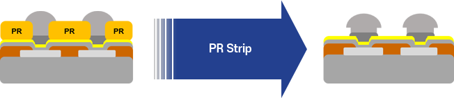
- Metal 손상 및 PR 잔류물 없이 thick PR을 제거하는 것이 가능함
- 공정 Type에 따른 수계, 유기계 선택 가능
- Low Metal Damage (Cu, Ni, Sn, Ag, Al)
- PR 종류, 두께에 따른 Strip 성능 구현 가능
Cu / Ti Etchant
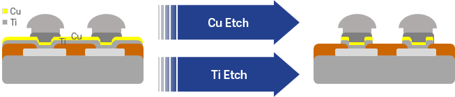
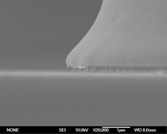
Cu Etchant
- Etching Uniformity 및 선택적 식각력 우수
- 광범위한 Etch Control 가능 (30Å/s~200Å/sec)
- Low Metal Damage (Ag, Sn, Ni, EP-Cu)
Ti Etchant
- 비불화물 계열로 Ti, Ti/W 의 선택적 식각이 우수
- H₂O₂ 혼합 비율에 의한 Etch Rate Control이 가능 (5Å/s ~ 22Å/sec)
Au Etchant
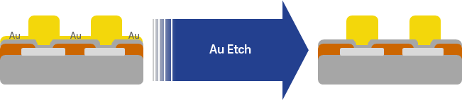
- 요오드 계열의 식각액으로 Au metal에 대한 선택적 에칭이 용이함
- Low Metal Damage (Al)
- 우수한 소재안정성 확보 Etching Uniformity 우수 누적매수, lifetime 우수