개별 칩들을 단일 패키지로 결합시킨 초박형, 고집적 토탈 패키징 솔루션입니다.
nSiP Solutions
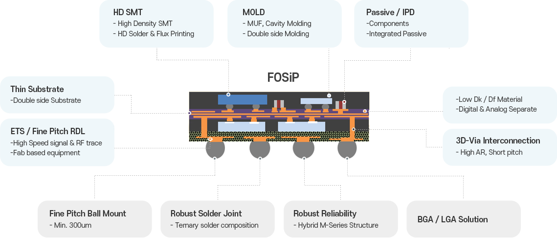
SiP is wafer level & chip last(RDL first) based System in Package solution where multi RDL & double side mounting is possible.
nSiP(nepes SiP) offers more compact & slimmer feature compared to substate base SiP
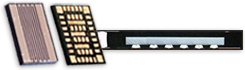
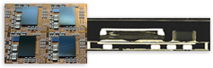
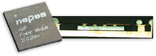
Product View
| VALUE | FC & High I/O FC | 2D | 3D system level | |||
|---|---|---|---|---|---|---|
| xfBGAn | nSiP_2.xD | RF-SiP | AiP | SL-nSiP | power module | |
| Product View |  |
 |
 |
 |
 |
 |
| Advantages |
Extremely thin profile up to No limited fan out routing ratio |
2.3D RDL interposer & 2.1D RDL |
Ultra high density extreme thin |
mmWave & Cm scale antenna |
3D analog and digital function |
Thermally enhanced high |
| Features |
Thinner profile & Minimum Footprint Cost competitive solution High yield & Turnkey solution |
Thinner substrate with higher I/O Large body with warpage |
Multiple active electronic Multiple functions associated with |
Package-level antenna integration Small form factor & design |
Improved electrical performance High I/O capability and small form |
Reduced cost by replacing carriers High input/output current |
| Application | Communication Consumer, Automotive, Industrial, (RFFE, Wireless connectivity, mmWave, Wearable, Sensor, Power, IoT) |
|||||
Address충청북도 청주시 청원구 오창읍 과학산업2로 587-32
Tel043-240-8500(내선2번)