IT Chemical for Semiconductor & Display
We provide global leading companies with cutting-edge polymerized lithography materials
and functional wet chemicals that are applied to the manufacturing processes of semiconductor
and display devices to be adopted in smart phones, cars and other IT devices.
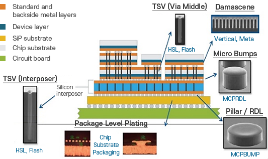
Semiconductor Process
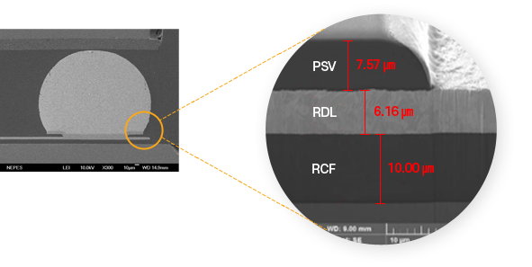
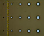
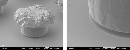
Organic Insulator
- Product Name
- NDP-series
- Characteristics
- It is designed to be cured at low temperature, so it has low shrinkage, low dielectric constant, high resolution, excellent thermal stability and chemical resistance.
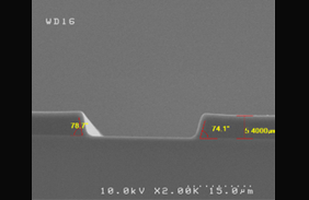
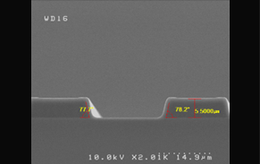
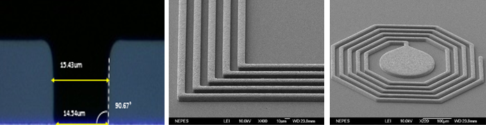
- Structure
| unit | NDP-series | |
|---|---|---|
| Cure | ℃ | ≤ 200 |
| Shrinkage | % | ≤ 1 |
| Water Absorption | % | ≤ 1 |
| DK (Dielectric Constant) | 25 GHz | < 3.0 |
| DF (Dissipation factor) | 25 GHz | < 0.02 |
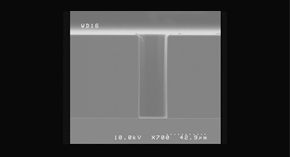
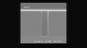
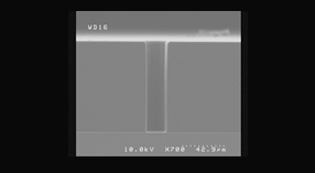
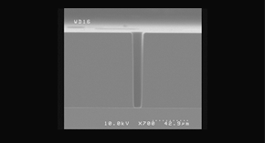
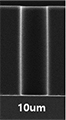
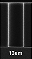
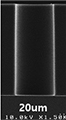
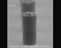
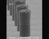
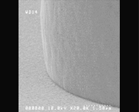
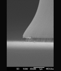
| Line/Space | Hole | Line/Space | ||||
|---|---|---|---|---|---|---|
| 25㎛ | 20㎛ | 25㎛ | 20㎛ | |||
| THK 5㎛ |
 |
 |
 |
 |
||
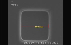
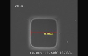
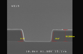
| CD/Taper/THK | 25.5㎛ | 20.3㎛ | 76.4˚ | 5.4㎛ | 78.0˚ | 5.5㎛ |
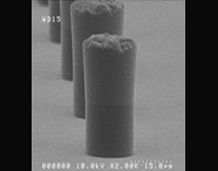
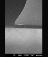
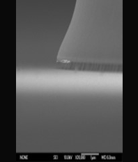
| THK 10㎛ |
 |
 |
 |
 |
||
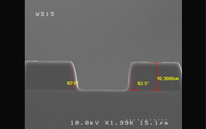
| CD/Taper/THK | 23.4㎛ | 18.1㎛ | 78.5˚ | 10.2㎛ | 82.6˚ | 10.3㎛ |
Developer for Organic Insulator
- Product Name
- NOD-01
- Characteristics
- A product with excellent low/high-temperature insulation film and process margin
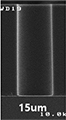
| After Dev. (Top size) |
NOD-01 | NOD-01 | ||
|---|---|---|---|---|
| 20sec X 3puddle |
≥ 20um open |
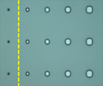 |
≥ 15um open |
 |
| 35sec X 3puddle |
≥ 20um open |
 |
≥ 15um open |
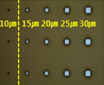 |
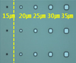
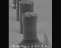
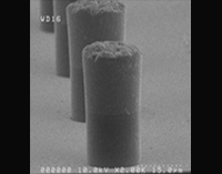
Photoresist
- Product Name
- Nega PR
- Characteristics
- A product with excellent low/high-temperature insulation film and process margin
Nega PR : NNBP-103T, NUTP-264
| NUTP-264 | 90um Octagonal Pattern | 80um Octagonal Pattern | 70um Octagonal Pattern | 60um Octagonal Pattern |
|---|---|---|---|---|
|
Octagonal Pattern Exposure Energy : 1000mJ/cm2 Focus : -5.0um |
 |
 |
 |
 |
| 50um Octagonal Pattern | 40um Octagonal Pattern | 35um Octagonal Pattern | 30um Octagonal Pattern | |
 |
 |
 |
 |
|
| 25um Octagonal Pattern | 20um Octagonal Pattern | 15um Octagonal Pattern | 10um Octagonal Pattern | |
 |
 |
 |
 |
- Product name
- Posi-PR (NPIH-series)
- Characteristics
- A product with high limiting resolution, excellent chemical resistance, plating resistance, and process margin
| Patterned on Cu wafer | Plated on Cu wafer |
After PR Strip | |||
|---|---|---|---|---|---|
 |
 |
 |
 |
 |
 |
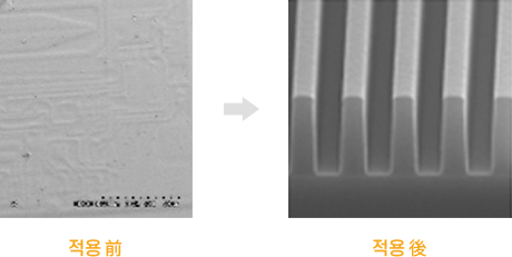
Developer for Photoresist
- Product name
- CPD-series
- Characteristics
- A high-purity product that enables the creation of micro patterns in a semiconductor through the development process following a cutting-edge micro semiconductor lithography process
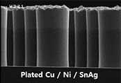
Cu Electroplating
- Product name
- Damascene-series
- Characteristics
- Applicable to plating equipment (Lam, applied materials, TEL, Ebara)
PR Stripper
- Peoduct Name
- BMS-series
- Characteristics
- Photoresist & negative aqueous stripper with broad process margin, eco-friendly material, and zero metal damage
| Mask | 300sec(PR Residue) | 350sec(PR Residue) | 450sec(No PR Residue) | 550sec | 1800sec | 3600sec |
|---|---|---|---|---|---|---|
| BMS- 850W |
 |
 |
 |
 |
 |
 |
 |
 |
 |
 |
 |
 |
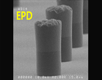
Metal Etchant
- Peoduct Name
- BCE, BTE, GME-Series
- Characteristics
- Excellent control of etching time and amount, excellent process margin
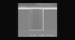
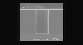
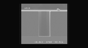
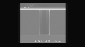
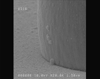
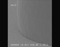
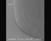
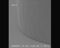
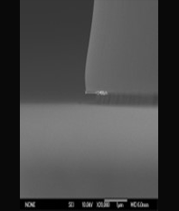
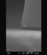
Cu Etchant : BCE-Series
| BCE-131B | BCE-131C | BCE-131H | ||||
|---|---|---|---|---|---|---|
| EPD | Over time (50 %) | EPD | Over time (50 %) | EPD | Over time (50 %) | |
| SEM Image |
 |
 |
 |
 |
 |
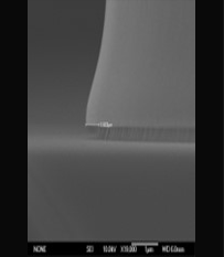 |
| E/Time (sec) | 100 | 150 | 70 | 105 | 25 | 38 |
| Under cut (㎛) | 0.3 | 0.5 | 0.3 | 0.47 | 0.3 | 0.5 |
| Etch Rate (Å/sec) | 30.0 (@ 23℃) | 42.9 (@ 23℃) | 120.0 (@ 23℃) | |||
nepes corp.
Address105, Geumil-ro 965beon-gil Samseong-myeon, Eumseong-gun, Chungcheongbuk-do
Tel+82-43-877-3040
E-mailsalesem@nepes.co.kr