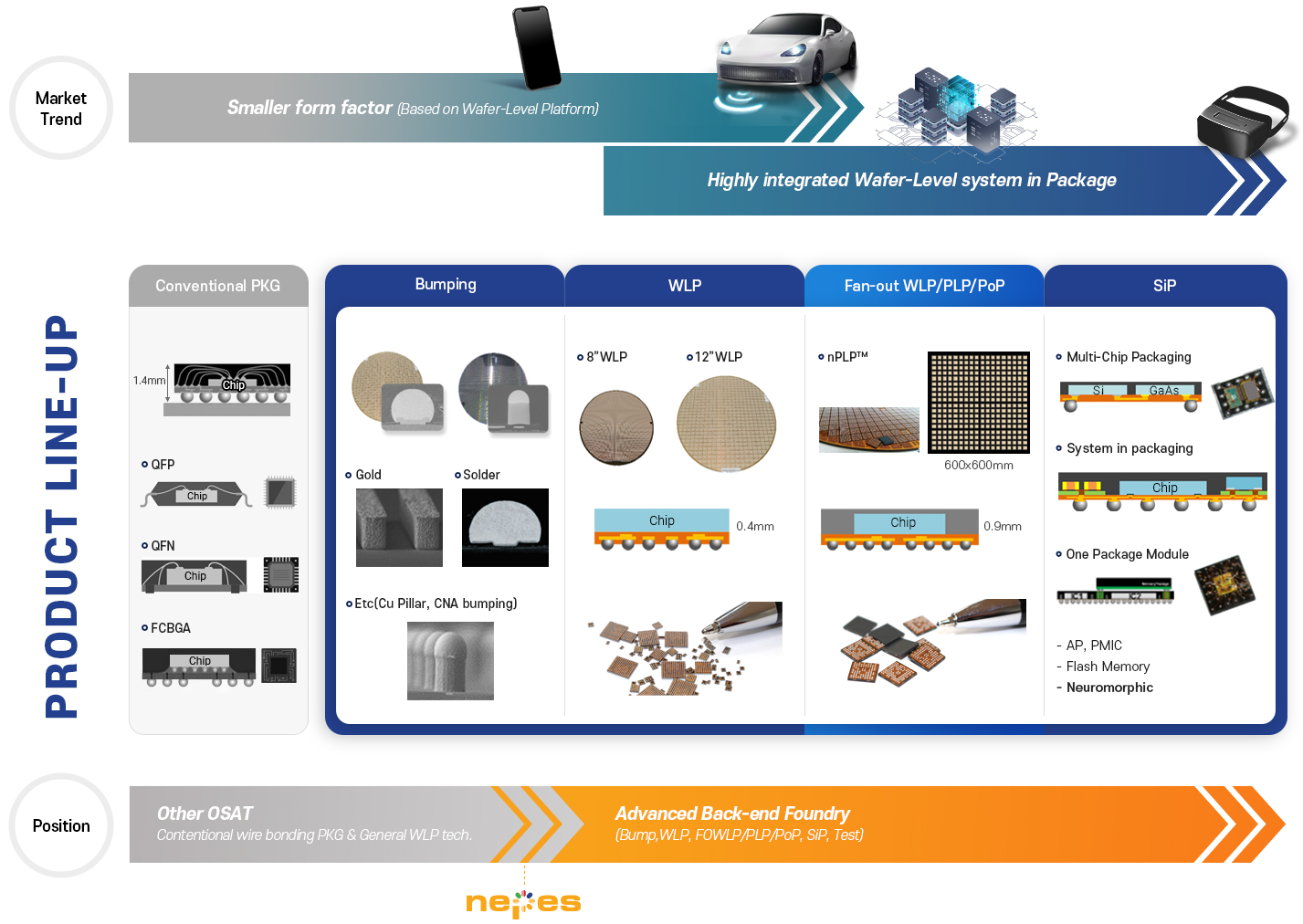
Full Turn-key Solutions of
Bumping, WLP, FOWLP/PLP, SiP and Test
nepes is a leading-edge provider of Wafer Level Packaging, providing full turnkey solutions that include 8” & 12” Flip-chip bumping
and Test nepes provides an extensive range of packaging options such as, WLCSP, FOWLP/PLP/PoP, SiP as well as 2.5D/3D
modules without conventional substrates. nepes has also been the first 600mm x 600mm Fan-Out PLP OSAT in the world in high
volume production since September 2021, and strengthened its Fan-Out packaging portfolio by licensing M-Series™.
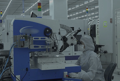
nepes operates Back-end foundry in Korea, Philippines, China to meet the dramatically increasing demand of advanced packages
from global fabless and IDM customers with innovative packaging leadership.
Watch more
nepes’ semiconductor market positioning