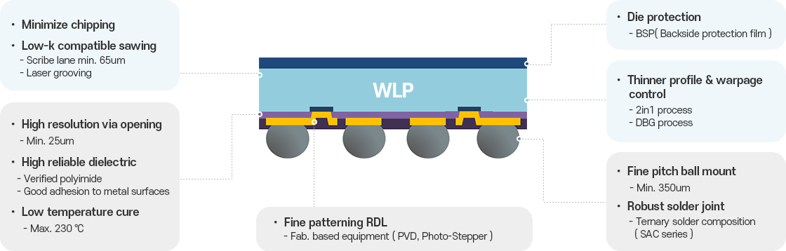
Wafer Level Package (WLP)
An optimal cutting-edge packaging solution for lighter, thinner, shorter,
and smaller chips, processing bumping and RDL without cutting the wafer.
Wafer Level Packaging Solutions
nepes Wafer Level Package (WLP) portfolio includes wafer bumping, wafer level probe test to support full turn-key solutions
nepes provides low cost solution with high reliability/technology to meet the dramatic demand in various applications
Product View
| VALUE | FIWLP |
|---|---|
| Product View |  |
| Wafer Size | 200mm & 300mm |
| Advantages | ▣ Meets JEDEC MSL1 CLR and BLR requirements |
| Features |
|
| Application | Communication, Consumer, Automotive, (PMIC, DC converter, Wireless charging IC, Display/Driver IC, Audio Codec, Transceivers, Connectivity Module) |
nepes corp.
Address587-32 Gwahaksaneop 2-ro Ochang-eup, Cheongwon-gu, Cheongju-si, Chungcheongbuk-do
Tel+82-43-240-0500 (Line 3)
E-mailsales@nepes.co.kr