To provide high functional materials
to next generation nano-device
Negative Photoresist

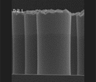
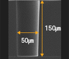
Negative Thick photoresist for Wafer Level Package - RDL, CPB
-
Cu RDL (Redistribution Layer)
- PR pattern
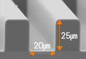
- Cu RDL
-
CPB (Cu Pillar Bump)
- PR pattern
- CPB
- Securing polymer and formulation design technology
- Excellent pattern profile (no footing, no under-cut)
- Excellent process margin
- Fast processing
- High resolution
- High plating resistance
Positive Photoresist
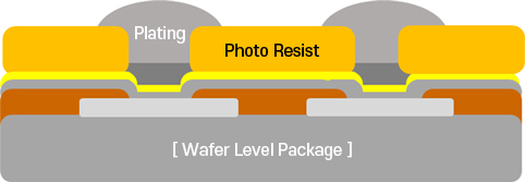
Positive Thick photoresist for TSV, CPB
-
TSV (Trough Silicon Via)
- PR pattern
- Plating
-
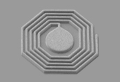
CPB (Cu Pillar Bump)
- PR pattern
- Plating
-
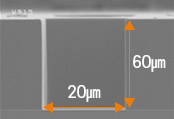
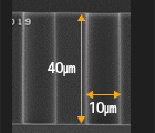
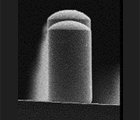
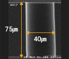
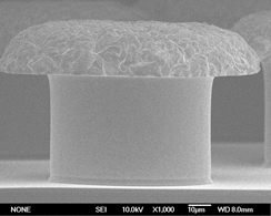
Tall Pillar
- PR pattern
- Our own polymer design and optimized Formulation
- Excellent pattern profile (no footing, no under-cut)
- Excellent strip ability (no residue)
- High resolution / aspect ratio
- Wide process margin
- Excellent chemical & plating resistance
Photo-definable Dielectiric
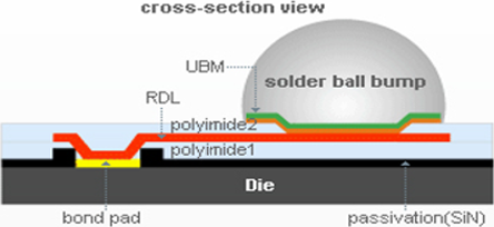
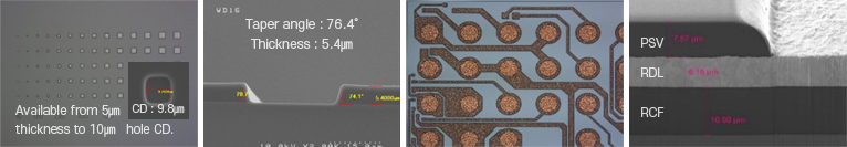
Photo-definable dielectric for advanced package
- NDP-Series used as various protection/insulation layers in the bumping process
- Soluble Polyimide backbone: Ultra-low-temperature cure, ultra-low shrinkage
PR Stripper
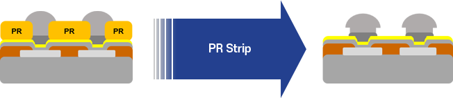
- It is possible to remove the thick photoresist without metal damage and residue
- An aqueous or organic type stripper can be selected according to the photo process conditions
- Low Metal Damage (Cu, Ni, Sn, Ag, Al)
- Strip performnce can be controlled according to the type of PR and thickness.
Cu / Ti Etchant
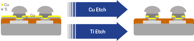
Cu Etchant
- Excellent etching uniformity and selective etch rates
- Wide-range etch control (30Å/s~200Å/sec)
- Low Metal Damage (Ag, Sn, Ni, EP-Cu)
Ti Etchant
- Excellent selective etching of Ti, Ti/W with non-fluoride series
- Etch rate control by H₂O₂ mixing ratio is possible (5 ~ 22Å/sec)
Au Etchant
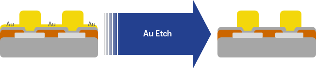
- Excellent etching uniformity of Au (gold) metal with iodine based etchant
- Low Metal Damage (Al)
- Securing excellent material safety Excellent etching uniformity Exellent Number of throughput & Bath Lifetime