-
 NEWS
NEWS
-
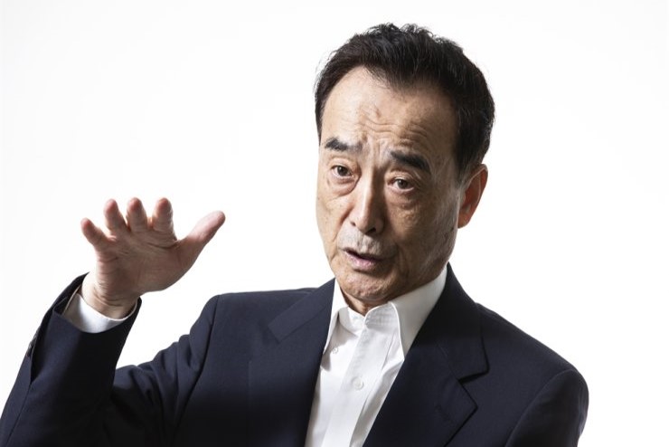
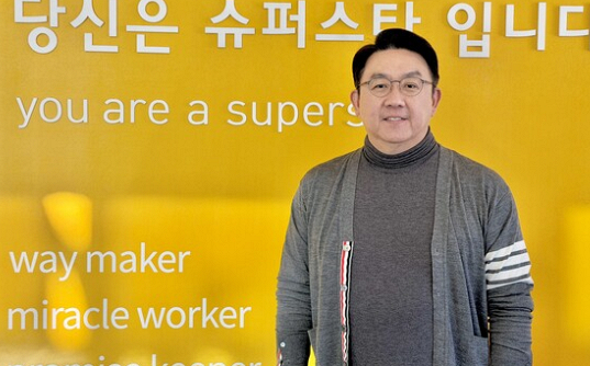 Nepes Vice President Ahn Jung-ho Emphasizes the Need for an Inclusive AI Education Environment
Ahn Jung-ho, Vice President and Chief Information Officer (CIO) leading the Digital Education Business at Nepes, recently emphasized the importance of public education keeping pace with rapid technological change in the era of artificial intelligence (AI), according to a media interview.Building on its core semiconductor technology capabilities, Nepes has expanded into the education sector by developing and operating customized AI-driven learning solutions and educational content through its AI and digital education brand, kocoaFab. These initiatives are designed to support personalized learning by reflecting individual students’ learning levels and environments, while also contributing to teacher training programs and public education projects.Nepes is particularly focused on creating an inclusive AI education ecosystem that reaches underserved student groups. By leveraging accessibility-enhancing technologies such as voice-based AI educational tools, the company aims to ensure broader participation in AI-enabled learning. Nepes also plans to further develop AI education models validated in Korea into scalable global reference models. Vice President Ahn noted that the core of AI education lies not in technology itself, but in people and the transformation of learning environments. He reaffirmed Nepes’ commitment to building an AI education framework in which all students can benefit from technological advancement without experiencing educational or digital divides.Original Article▶ ChosunBiz Ahn Jung-ho, Vice President of Nepes: “We Must Create an AI Education Environment for Everyone” (December 31, 2025) Read the full article: [Link to original article]
2026-01-14 -
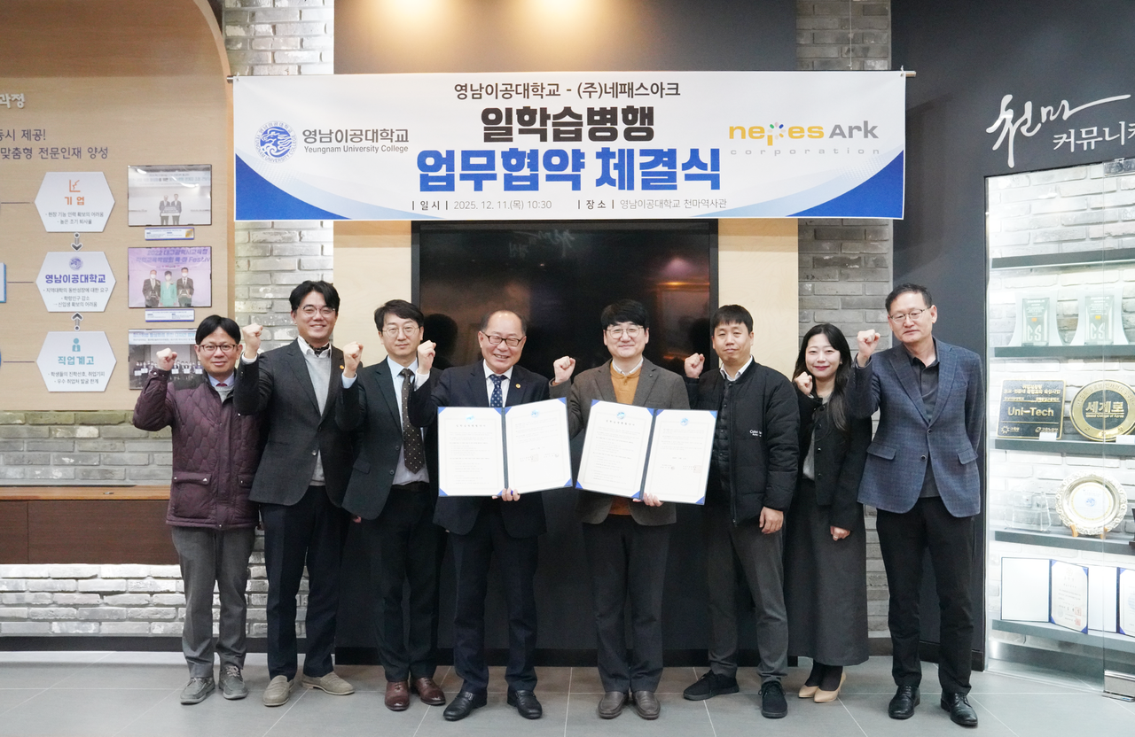 Nepes Ark Signs Work-Study Partnership Agreement with Yeungnam University College in Semiconductor T
On December 11, Nepes Ark, a leading semiconductor testing company, signed an Industry-Academia Cooperation Agreement for Work-Study in Semiconductor Testing at Cheonma History Hall of Yeungnam University College.This agreement aims to systematically foster field-ready professionals in the critical semiconductor testing sector and expand employment opportunities for young talent. Attendees included Sang-woong Ma, Executive Director; Seong-ho Yoon, Principal Engineer; and Seong-dae Bae, Senior Engineer from Nepes Ark, along with Jae-yong Lee, President of Yeungnam University College; Geum-gil Seong, Director of Career Support; Chang-hwan Kim, Head of Work-Study Support Center; and Seung-hyun Jeong, Head of ICT Semiconductor Department.Through this partnership, both organizations plan to collaborate in various areas, including ▲Strengthening industry-academia networks ▲Developing customized corporate training and professional talent ▲Linking employment opportunities for graduates of semiconductor testing programs ▲Creating and operating work-study-based curriculaNepes Ark aims to establish a practical industry-academia cooperation model that organically connects education and recruitment, taking the lead in nurturing professionals with the expertise and hands-on skills required in the semiconductor industry.[Photo courtesy of Yeungnam University College][Request to add press release distribution list]
2025-12-19 -
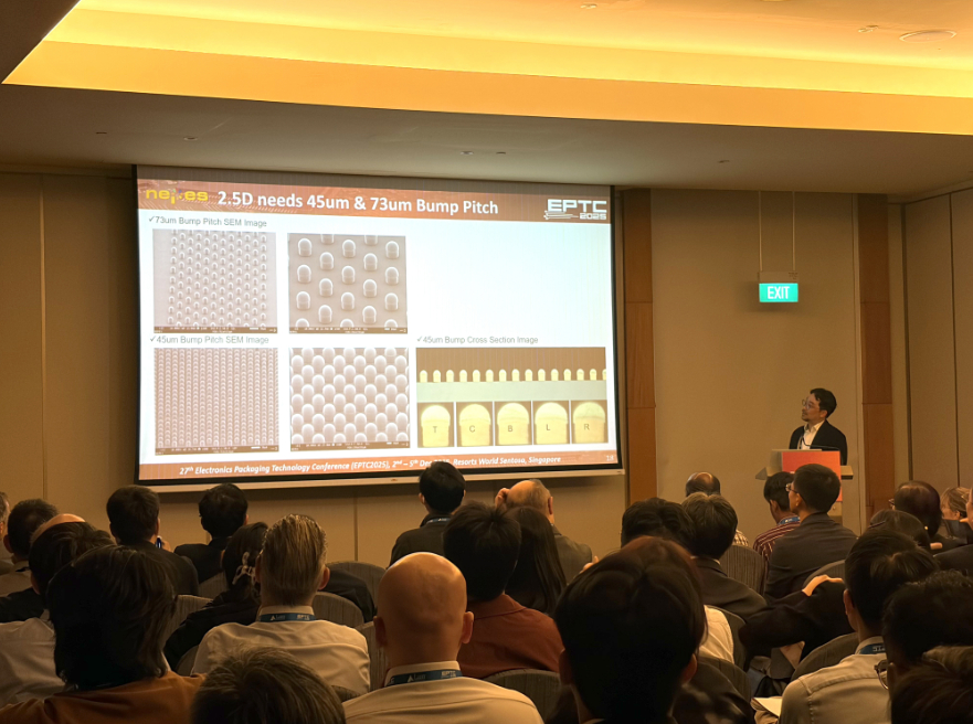 Nepes Presents Next-Generation Interposer Technology at Global Semiconductor Packaging Conference EP
Nepes participated in the IEEE Electronics Packaging Technology Conference (EPTC 2025), held in Singapore from December 2 to 5, and presented its research results under the theme “Development of Embedded Bridge Die Interposer Using Fan-out Packaging for Heterogeneous Integration of NPUs and HBMs.”EPTC is a prestigious international conference in the Asia-Pacific region on semiconductor packaging and heterogeneous integration, organized by the IEEE Electronics Packaging Society (EPS). Leading global semiconductor companies and research institutions such as ASE, Amkor, TSMC, IMEC, and A*STAR take part in this event to share the latest technology trends.The presentation addressed the growing need to densely integrate NPUs and HBMs within a single package for HPC and AI systems, introducing an Embedded Bridge Die Interposer technology based on FOWLP (Fan-Out Wafer Level Packaging) to overcome the limitations of conventional silicon interposers. The institute showcased its in-house developed process flow, including wiring formation and die bonding, along with prototype samples, highlighting the scalability of fan-out technology.This year’s conference mainly featured topics on heterogeneous integration technologies, including hybrid bonding, and materials, providing insights into the global research and industry directions. Through this, Nepes reaffirmed the need to further strengthen follow-up process development and reliability evaluation for its ongoing 2.5D and edge computing technologies.[Request to add press release distribution list]
2025-12-19 -
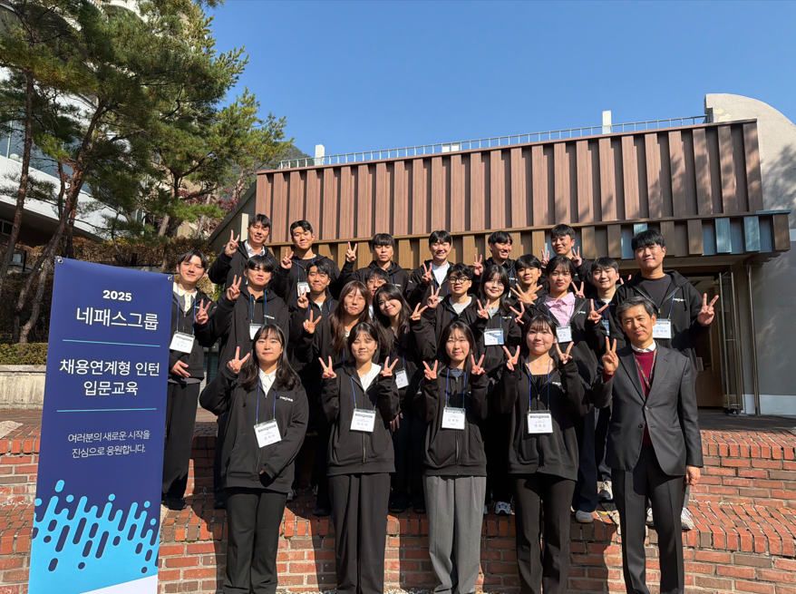 Nepes Successfully Completes Introductory Training for 2025 Recruitment-Linked Interns
Nepes announced that it successfully completed its introductory training program for recruitment-linked interns, held from November 3 to 7. A total of 21 interns participated in the program, beginning their journey to become future core talents across all departments of the Semiconductor Business Division.The training was systematically designed and executed with the goals of embedding organizational vision and core values, strengthening AI-driven practical skills, and building understanding of key job roles. In particular, the program was structured around three pillars: Organizational Fit × AI-Driven × Skill-Up, enabling interns to quickly adapt to Nepes’ culture and acquire essential competencies for on-the-job success.The curriculum included: Understanding Nepes’ corporate culture and vision Learning AI and semiconductor industry trends Mandatory environmental and safety training Core job academies (Technology, Quality, Integrated Operations Management) Following this, interns will undergo a three-week advanced job academy to further enhance their practical application skills.Participants expressed high satisfaction with the program, demonstrating strong engagement and proactive communication. Many developed concrete action plans for applying their learning to real work scenarios, laying the foundation for future conversion to full-time positions. A Nepes representative stated: “This introductory training was more than just knowledge transfer—it provided a meaningful foundation for interns to grow as integral members of Nepes’ future. We will continue to actively support their smooth integration and capability development within the company.”[Request to add press release distribution list]
2025-11-19 -
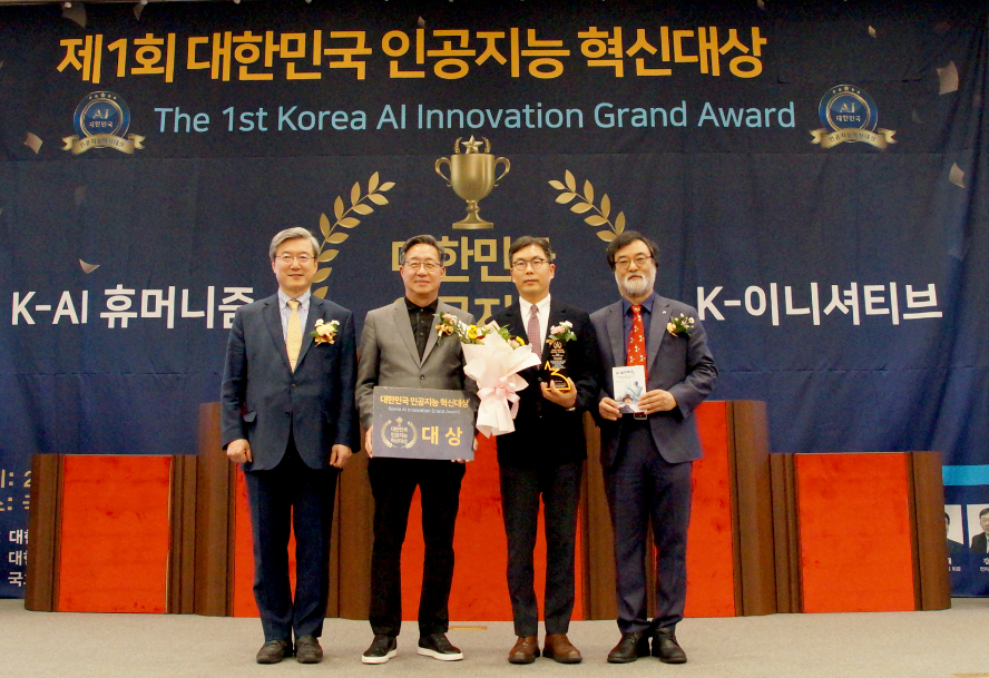 Nepes Wins Grand Prize in AI Education Innovation at Korea AI Innovation Awards 2025
Leading the Education Ecosystem Through AI-Based Public Education Innovation and Digital InclusionNepes received the Grand Prize in AI Education Innovation at the 2025 Korea AI Innovation Awards held on November 10. This event is a leading AI awards ceremony in Korea, organized by the Korea AI Innovation Awards Committee, co-hosted by the International Future Society, ET News, the National Assembly Future Policy Research Association, and the Korea AI Forum, and supported by major government ministries including the Ministry of Science and ICT and the Ministry of Trade, Industry and Energy. Under the theme of “K-AI Humanism and Innovation,” the awards recognize companies and institutions that have contributed to industrial innovation and the realization of social value through AI technology.For more than a decade, Nepes has spearheaded educational innovation by integrating AI and digital technologies, contributing to the development of Korea’s AI education ecosystem based on a human-centered educational philosophy.Since 2013, Nepes has provided AI education to over 120,000 students and teachers annually through initiatives such as: Development of AI educational products and content Research on human-AI collaborative learning models Execution of government public education projects AI education programs for underserved communities In particular, Nepes partnered with tech company IoTed to develop “AI Geumjjogi,” a ChatGPT-powered voice-recognition AI educational speaker that helps elementary and special-needs students enhance problem-solving skills. The company also collaborated with Seoul National University to academically validate and conduct pilot studies on human-AI collaborative learning models.Furthermore, Nepes promotes personalized learning through a generative AI-based learning platform and operates “CocoaFab School,” a teacher community with over 5,600 active educators, driving digital transformation in classrooms.Beyond public education innovation, Nepes develops AI ethics education content, runs the “Digital Hero” project-based learning program focused on solving social issues, and engages in CSR activities to support marginalized groups such as students in remote areas and multicultural families—fulfilling its commitment to public value and social responsibility.A Nepes representative stated: “As a semiconductor packaging innovation company that turns an AI-driven future into reality, we will continue to lead efforts to create a better society through AI technology in education.” This award recognizes Nepes’ contributions beyond technological innovation—addressing educational gaps, promoting digital inclusion, and advancing ethical AI practices as part of its social value mission.[Request to add press release distribution list]
2025-11-19 -
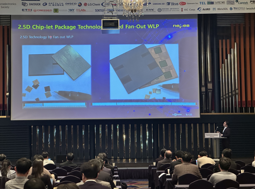 Nepes Presents Next-Generation AI Semiconductor Packaging Technology at ISMP 2025
Nepes successfully delivered a presentation titled “Fan-Out Embedded Bridge Interposer for Scalable Heterogeneous Integration of NPUs and HBMs” at ISMP 2025 (23rd International Symposium on Microelectronics and Packaging), held from November 4 to 7 at the Inter-Burgo Hotel in Daegu.The presentation showcased Nepes’ achievements in developing fan-out-based bridge interposer technology for heterogeneous integration of AI processors and high-bandwidth memory (HBM). Attendees praised the session for offering practical solutions to achieve high-density, high-speed, and low-power packaging.ISMP 2025 is an international symposium spotlighting advanced packaging technologies such as 3D/2.5D integration, chiplet-based design, hybrid bonding, and UCIe interfaces. This year, numerous sessions focused on AI semiconductors and next-generation memory integration. Leading global semiconductor companies—including Intel, Samsung Electronics, SK hynix, Lam Research, Tokyo Electron, PulseForge, and Samsung Electro-Mechanics—participated as presenters, alongside academic experts from UCLA, USC, and KAIST, fostering active technical exchange and collaboration.Through this presentation, Nepes emphasized the design flexibility advantages of its proprietary Fan-Out Embedded Bridge Interposer technology and highlighted its potential applications in high-performance domains such as AI servers, edge computing, and autonomous vehicles.Jungwon Lee, Director of Nepes Semiconductor Research Center and presenter of the session, stated:“Our ISMP 2025 presentation was an opportunity to demonstrate Nepes’ efforts not only in RDL interposer development but also in securing Fan-Out Embedded Bridge Interposer technology. We will continue to lead innovation in AI semiconductor packaging as a representative of Korean companies.”[Request to add press release distribution list]
2025-11-19 -
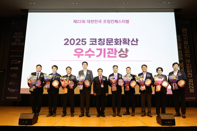 Nepes Wins Excellence Award at Korea Coaching Festival 2025
Driving People-Centered Organizational Culture Innovation… Recognized for Spreading Coaching Culture to Manufacturing SitesNepes received the 2025 Excellence Award for Coaching Culture Expansion at the 22nd Korea Coaching Festival, held on October 31 at COEX in Seoul. This award, presented annually by the Korea Coach Association, honors organizations that contribute to the spread of coaching-based organizational culture. Nepes was highly evaluated for practicing coaching leadership based on its people-centered management philosophy and the GRACE model.As a mid-sized company located in Cheongju, Chungbuk, Nepes has drawn attention for its strong execution in spreading coaching culture within the industry through field-oriented training programs. Since December 2024, more than 10% of all employees have participated in on-site coaching education, with 130 employees completing the program so far and over 160 expected by year-end. Among them, 19 have earned KAC certification and 2 hold KPC credentials, demonstrating a commitment to embedding coaching leadership beyond simple training through official certification.Additionally, Nepes collaborates with professional coaches to run the “Coach the Coach” program, fostering a self-sustaining coaching ecosystem in regional industrial sites. Between 2024 and 2025, a total of 60 participants engaged in the program, working with 22 professional coaches to conduct over 200 coaching sessions—creating a culture where coaching is practiced in everyday work.Nepes’ organizational culture is built on the GRACE model (Growth, Respect, Assistance, Conditions, Empathy), with a particular focus on Empathy. The company supports all members of its Empathy organization in obtaining KAC certification, enabling psychological safety and deep communication. These members are responsible for counseling, listening, and care, effectively implementing the company’s people-centered management philosophy.The impact of this coaching culture is evident in measurable improvements in organizational engagement and leadership capability. For example, the “Communication” score rose from 4.41 in 2023 to 4.75 in 2024, “Supervisor Leadership” improved from 5.31 to 5.56, and “Coaching Feedback” continues to show steady progress.The event featured a keynote speech by Professor Dae-Shik Kim of KAIST and a special lecture by Dr. Carlos Davidovich from Harvard Medical School’s affiliated Coaching Institute, along with case studies in education, HR, youth, and life coaching. Nepes demonstrated its philosophy of prioritizing human growth and connection even in technology-driven industries, presenting a sustainable organizational growth model through coaching.Nepes’ award representative, Lee Sang-ho, Head of Management Support, stated:“Even in the AI era, a people-centered organizational culture is the core of competitiveness. This award is a recognition of Nepes’ philosophy of respecting people.”Meanwhile, this year’s Excellence Award for Coaching Culture Expansion was granted to 21 organizations, including Nepes, HD Hyundai Group, KT Cloud, KakaoBank, and Hanwha Aerospace.[Request to add press release distribution list]
2025-11-19 -
 35 Years of Walking Together, 100 Years of Leaping Forward: Nepes Declares Its Future Management Vis
To mark its 35th anniversary, Nepes held a commemorative event with employees at the Cheongju 2 Campus Atrium, reflecting on its journey over the past 35 years and sharing its management philosophy and vision for the next 100 years.Chairman Byung-Koo Lee delivered a keynote message under the theme “35 Years of Walking Together, 100 Years of Walking Forward Together,” presenting three core principles for future management: Mission-driven growth Spiritual management to achieve vision Strengthening competitiveness through collective intelligence Chairman Lee stated, “Over the past 35 years, Nepes has achieved remarkable growth by continuously innovating and developing technologies tailored to the needs of domestic semiconductor customers, delivering them in a timely manner.” He emphasized that this growth was not merely technology-driven, but the result of realizing customer-centered value.He further added, “Moving forward, a culture of horizontal communication, collaboration, respect for diversity, and a fearless spirit of experimentation—where we think together, decide together, and take responsibility together—will be the driving force that leads Nepes to become a centennial company.” In addition, the event served as a platform to reinforce the company’s commitment to combining community spirit with AI-driven strategic execution. Under the 2026 slogan “All hands on the AI Core,” Nepes announced its plan for all employees to unite their efforts in proactively responding to the evolving industrial landscape.[Request to add press release distribution list]
2025-10-24 -
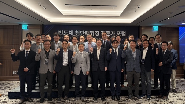
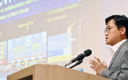 Nepes Presents Growth Strategy for Mid-Sized OSAT Companies at Semiconductor Packaging Policy Forum
Nepes participated in the Semiconductor Packaging Policy Forum held on September 25 at the SC Convention Center in Seoul, where CTO Jongheon Kim delivered a keynote presentation titled “Growth Strategy for Mid-Sized OSAT Companies and Industry-Academia-Government Collaboration.”In his presentation, Mr. Kim addressed the limitations of 2.5D packaging (CoWoS), a core technology in the AI semiconductor market, and stated, “In the future, packaging technologies that replace expensive silicon interposers and shift to square panel formats will gain attention.” He added, “The industry is already discussing 3.5D packaging technologies that incorporate vertical stacking, and companies that secure next-generation technologies and build robust supply chains will lead the market.”Mr. Kim also outlined strategic directions for enhancing the competitiveness of mid-sized OSAT companies, including:Customer-driven technology development,Proactive supply chain establishment, andTimely response to advanced packaging technologies.Furthermore, he emphasized the need for government policy support and increased investment to help mid-sized OSAT companies strengthen their technological capabilities. In particular, he highlighted the importance of public sector involvement in the commercialization of advanced packaging technologies and the establishment of evaluation infrastructure for materials and equipment.The forum, hosted by the Korean Microelectronics and Packaging Society (KMEPS), brought together experts from industry, academia, and research institutions to discuss the future of advanced packaging and policy directions. Through this presentation, Nepes reaffirmed its leadership in the industry by offering practical insights into growth strategies and ecosystem collaboration for mid-sized OSAT companies.Related Article: [Semiconductor Packaging Policy Forum] Industry Says “Paradigm Shift Requires New Technology and Market Strategies” – ETNews
2025-09-26 -
 Nepes Expects Turnaround Driven by Demand for AI Server-Used Power Semiconductors - Daishin Securiti
- Based on 2024 sales (KRW 460 billion), semiconductors accounted for 71%, electronic materials 17%, and rechargeable batteries 11%.- The semiconductor division primarily derives revenue from WLP (Wafer Paper Packaging), a high-value-added packaging product.- While the company is the only company in Korea capable of mass-producing FOPLP packaging, it was classified as a discontinued business in 2024 due to significant losses, aiming to stabilize its financial structure.- The upstream market for its core business, WLP, is expanding from smartphones to AI servers. In April 2025, the company decided to expand its packaging line for AI semiconductors.- Sales of Cu plating solutions for electronic materials, HBM, are expected to continue to grow in 2025, and the rechargeable battery division is also expected to turn around with recovering lead tab performance.Source: "Turnaround Expected Driven by Demand for AI Server-Used Power Semiconductors" Naver Pay Securities
2025-08-27 -
![[Report] Nepes, a Key Material, Part, and Equipment Company, Returns to Korea…Fitting Up the Supply 썸네일](https://www.nepes.co.kr/data/bbsData/17560882629.jpg) [Report] Nepes, a Key Material, Part, and Equipment Company, Returns to Korea…Fitting Up the Supply
[Report] Nepes, a Key Material, Part, and Equipment Company, Returns to Korea…Fitting Up the SupplyThe Ministry of Trade, Industry and Energy announced on the 12th that Park Jeong-seong, Director of the Trade and Investment Office, visited the Cheongju plant of Nepes Co., Ltd., a semiconductor packaging manufacturer, to award certificates to companies returning to Korea. After hearing Nepes's investment plan, Director Park inspected the production site and the proposed investment site, listened to any challenges encountered during the repatriation process, and discussed government support measures for companies returning to Korea. Nepes is a comprehensive back-end foundry specializing in the complete supply chain for system semiconductors and possesses key strategic technologies for the material, part, and equipment sector. Nepes plans to expand its production facilities at the idle site of its Cheongju plant in North Chungcheong Province to expand its production capacity for domestic and international semiconductor companies. Amid accelerating global supply chain restructuring, the government is actively promoting the repatriation of cutting-edge and core supply chain companies to establish Korea as a global supply chain hub and stimulate domestic investment. Accordingly, Nepes' investment in the Cheongju plant is expected to contribute to the national economy by revitalizing the local economy through new jobs, expanding exports, and stabilizing the supply chain. Park Jeong-seong, Director of the Trade and Investment Office, emphasized, "The return of key materials, components, and equipment companies to Korea has significant economic benefits in terms of investment, employment, and exports, and is crucial for stabilizing the domestic supply chain." He added, "The return of leading companies like Nepes is particularly encouraging amidst intensifying global technological competition." He added, "The government plans to fully support the return of companies to Korea through institutional improvements." Inquiries: Overseas Investment Division, Investment Policy Bureau, Ministry of Trade, Industry and Energy (044-203-4069) [Source] Korea Policy Briefing (www.korea.kr)
2025-06-13
Investor Relations
NEPES, GLOBAL TOP-TIER PARTNER


![[DIC2024] Nepes Increases Production and Reduces Costs for FO Packaging 이미지1](https://www.nepes.co.kr/data/bbsData/17461609729.jpg)

![[Semiconductor Packaging Day 2022] Nepes expands the application area of FO-PLP. - ETnews 이미지1](https://www.nepes.co.kr/data/bbsData/16576096149.jpeg)

