Leading the new era with
cutting-edge semiconductor packaging solution
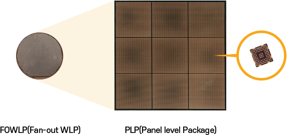
FOPLP
-

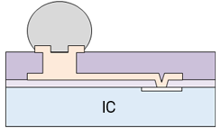
3D PoP Stackable( mPoP )
-

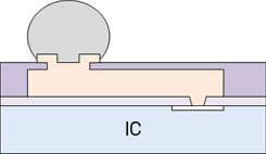
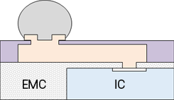
PoP( Package on Package )
-

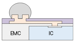
Multi-die( 2die )
-

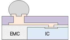
Chip-first( Face-up )
-

Chip-first( Face-down )
- A leading technology for next generation in the field of packaging
- Providing the high performance required for the 4th industrial revolution, including 5G and cloud data services
- Utilizing large square panel process in order to innovative productivity improvement and cost reduction beyond fan-out WLP process
- Advanced fan-out packaging technologies (MCP, mPoP, PoP) applicable to various markets and products, such as PMIC, RF module, APE, and memory
2.5D RDL interposer
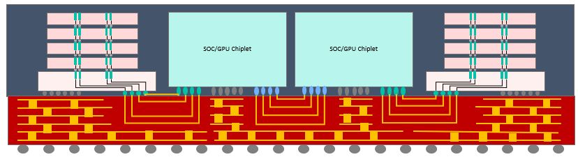
2.5D Chiplet
- Optimized for next-generation packaging requiring high interconnect density through u-bump with 73μm and 45μm pitches and 25μm diameters
- Fine-pitch(L/S 5/5μm and 2/2μm) enables precise circuit design that meets demanding layout requirements
- High-performance modules integrating NPU and HBM3 memory deliver exceptional data processing performance, ideal for AI and high-speed computing applications
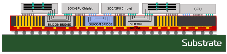
2.5D Chiplet
- Core technologies optimized for high-performance AI applications enable next-generation computing capabilities
- Designed to integrate AI accelerators and high-bandwidth memory for maximum processing efficiency
- Provides fine-pitch and high-density integration for scalable and powerful AI systems
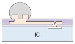
FOWLP/WLP
-
[nWLPRB]
-
[nWLPHR]
-
[nWLPHC]
-
[FOWLP]
-
[FOWLP]
-
[FOWLP]
- Creation of high-reliability, high-current WLP solution based on the differentiated technology of nepes
- Applicable to products in the fields of automotive, aerospace, and military along with the cutting-edge IT industry