Nepes, which eliminated semiconductor
leadframe, ‚Äúsemiconductor packaging efficiency 10 times‚Ķ Achieved 1 trillion won in sales within 3 years‚ÄĚ
Semiconductor manufacturing is divided
into a ‚Äėpre-process‚Äô, in which
a circuit is engraved on thin silicon to manufacture a chip, and a ‚Äėpost-process‚Äô, in which the manufactured
chip is packaged (packaging) using a substrate and metal wire.
Nepes a company specializing in
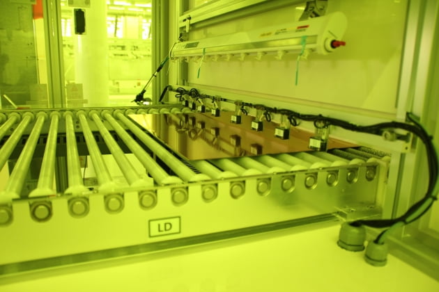
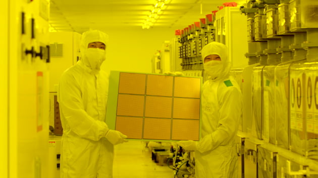
semiconductor backend-processing, recently started produce the 'Fan-out panel
level packaing'(FOPLP) that packaged high-performance semiconductors with a
thickness of 0.9nm and works in the form of a square panel(600mm)
It is the only technology in the world
that increases the net die (the number of chips per wafer or panel) more than
tenfold from 1,000 to 10,000. Since there is no wasted area on the edge of the
circular wafer, productivity is also greatly improved. Lee Byung-koo
(pictured), chairman of Nepes, said, “We are pushing
the semiconductor packaging technology to the limit through FOPLP and
others."
Nepes, a listed company on the KOSDAQ, is
a cutting-edge company in the packaging field. They mainly receive chips from
Samsung Electronics, etc., and package them to complete semiconductors. It has
the capacity to process 1104,000 wafers per year. Sales are 65% export and 35%
domastic. Last year, it recorded 418.4 billion won in sales and 16.4 billion
won in operating loss.
Nepes has been developing a technology
for packaging chips to be light, thin and short (light, thin, short and small)
so that semiconductors can be put into smartphones and IoTs. In the past,
semiconductors were shaped like a black centipede. Its size was much larger
than the chip. This is because the chip was placed on the board, a connection
part similar to a centipede was made using a copper wire, etc., and then an
epoxy resin was placed on it to fix it. Due to its complex structure, the heat
problem was also serious.
In contrast, the semiconductors packaged
by Nepes do not change significantly in the size of a square chip. This is
because they developed 'Wafer Level Packaging (WLP)' technology in the 2000s,
which coats a thin metal film just below the chip, prints a circuit diagram
with a laser, and sends and receives electrical signals using fine metal
protrusions. The thickness of the finished semiconductor was only 0.4 nm.
Overseas semiconductor manufacturers that have recognized Nepes' technology have
sent their chips by air to request packaging.
Nepes, which eliminated semiconductor
centipedes, “semiconductor packaging efficiency 10
times‚Ķ Achieved 1 trillion won in sales within 3 years‚ÄĚ
Nepes spares no expense in R&D and
facility investment to maintain cutting-edge technology. Last year, an
additional 42,962„é° factory site was prepared in Goesan,
North Chungcheong Province, and advanced packaging facilities such as WLP and
FOPLP were installed. Last year's operating loss is related to such facility investment.
Nepes'
earnings are expected to improve significantly this year. This is because the
total production capacity will increase by about 60% when the FOPLP facility
starts operation. The securities industry predicts that Nepes will record 606
billion won in sales and 52 billion won in operating profit this year. This is
almost twice as much sales as in 2020 (343.6 billion won).