
Jong Heon Kim, head of Nepes' Technology Development Division, gives a presentation on 'Trends and Role of Advanced Packaging Technology in High Performance Products'
at the '2nd DigitalDaily Industry Conference (DIC) 2024', held from 1:00 p.m. on November 21st at the Yeouido FKI Tower Conference Center Diamond Hall in Seoul, Korea .
[DigitalDaily reporter Kim Moon-ki]
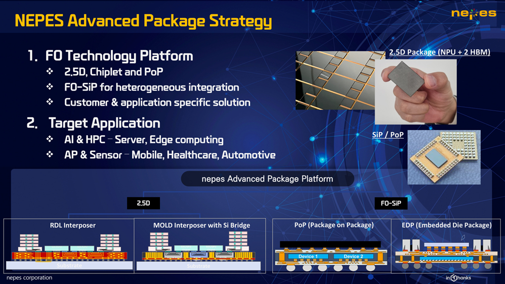
“Our continued efforts in packaging for the production of semiconductors in the AI era aim to increase production capacity. Nepes strives to bring not only productivity but also price competitiveness through fan-out (FO) packaging technology to silicon interposer. We will provide multiple services on a two-track basis, including technologies that cover 2.5D packaging and hold multiple chips in one package.”
Jong Heon Kim spoke about Nepes' competitiveness on the topic of 'Trends and Role of Advanced Packaging Technology in High Performance Products'. “The current semiconductor market resembles a war more than a strategy. As the market gradually localizes, we must focus on our strengths,” Kim said, adding that ”the same is true for the advanced packaging field.”
The pressure to follow Moore's Law is on, he notes. The curve of Moore's Law, which requires a doubling of scale every two years, has been bent. It costs around $500 million to design and test an existing chip and $30-40 million to produce a single wafer. Difficulties in manufacturing and prolonged periods of development, along with the high cost are proving to be a challenge.
“Packaging is the answer to physical limitations, manufacturing difficulties, and cost reduction,” said Kim. ”If there is a best practice in the construction of existing SoCs, we should follow it. Currently, chiplets are on the rise, as they can be divided by functions, in which simple processes and difficult processes are separated and put back together in the later stage of production."
Kim, however, points out that while silicon intensifiers offer high performance and efficiency in 2.5D packaging, they can be costly. An alternative is fan-out (FO) and wafer-level package (WLP) technology, which Nepes focuses on. This technology involves packaging chips on a wafer-by-wafer basis. It is advantageous for cost reduction as it eliminates the need for printed circuit boards (PCBs) and reduces the number of processes.

<source=nepes corp.>
<source=nepes corp.>
Kim also emphasized the need to foster the entire cycle of production from Front-end process to Back-end process.
“Even if the process is broken down into chiplets and put back together again, chip design and packaging must work together organically," he said. “In other words, it is important to build an ecosystem where the front and back are connected. In the end, the packaging and the chip must be designed together,” he said.
“It is said that Korea's competitiveness requires reviewing packaging from its beginning stage. We believe that there is potential and possibility to foster a whole ecosystem of AI semiconductors because we have AI data, foundries, and data-based platform companies," he said, adding, "Korea is also in dire need of technology collaboration."
[Source = DigitalDaily [DIC2024] 김종헌 네패스 “FO 패키징 ‘생산증가 원가절감’…韓 디자인-패키징 공급망 강화해야” - 디지털데일리]