「基板なし」が主流に
一方で、基板不足の影響を受けていないパッケ?ジ? 門メ?カ?もある。
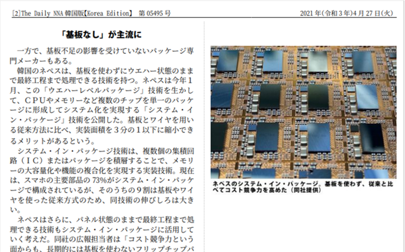
韓?のネぺスは、基板を使わずにウエハ??態のまま で最終工程まで?理できる技術を持つ。ネペスは今年1 月、この「ウエハ?レベルパッケ?ジ」技術を生かし て、CPUやメモリ?など複?のチップを?一のパッケ ?ジに形成してシステム化を?現する「システム?イ ン?パッケ?ジ」技術を公開した。基板とワイヤを用い る??方法に比べ、??面積を3分の1以下に縮小でき るメリットがあるという。
システム?イン?パッケ?ジ技術は、複?個の集積回 路(IC)またはパッケ?ジを積層することで、メモリ ?の大容量化や機能の複合化を?現する??技術。現在 は、スマホの主要部品の 73%がシステム?イン?パッケ ?ジで構成されているが、そのうちの9割は基板やワイ ヤを使った??方式のため、同技術の伸びしろは大き
い。
(the rest omitted)
"No board" is the mainstream.
There is a package maker where have not been affected by the shortage of substrates.
Nepes in Korea has the technology to process from wafer to packaging without using a substrate.
In January of this year, Nepes unveiled the "System in Package" technology by using "Wafer Level Package" technology.
"System in Package" technology forms a single package of multiple chips such as CPU and memory and realizes systematization.
It has the advantage of reducing the mounting area by less than one-third compared to the conventional method using a substrate and wire.
(the rest omitted)
[Source = Japan, The Daily NNA https://bit.ly/3eF8QzM]