-nepes announced
substrate-less SiP(System in Package) in the Electronic Components and
Technology Conference(ECTC)
-The
industry is giving attention to nepes SiP as an alternative solution for the
PCB replacement… Reliability test completed
Recently,
due to an unprecedented PCB shortage used for semiconductor packaging, the
market is interested in SiP solutions based on FOWLP and FOPLP technologies.
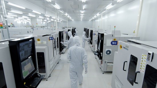
Nepes, the advanced
back-end foundry, promoted substrate-less SiP technology through ECTC and
started to target the market.
'nSiP
(nepes System in Package)', unveiled by Nepes, is a leading-edge technology of
the system semiconductor packaging roadmap. nSiP is based on ‘End-fab’ technology
without substrate and wire bonding and is the most optimized packaging solution for
high performance, high density, and small form factor. Also, nSiP is deployed
with redistribution layers on a chip instead of PCBs. It allows to reduce the
overall size of IC by 30 percent, the thickness by around 60 percent, and the
development period by more than 50 percent. The company recently released
sample products of packaging to customers across the globe.
While semiconductor manufacturers are having difficulties in launching and developing products due to a shortage of substrate and PCB supply, nepes is about to mass-produce FOPLP based on the End-fab technology. “The PLP and nSiP could meet growing demand for high-performing chips and components by providing a new solution for the need” said Kim Tae-hoon, President Corporate Marketing at Nepes. “It will also help relieve the chronic shortage of substrate in semiconductor industry,” he said.