-National project successfully completed... Optimization of manufacturing inspection equipment Deep learning acceleration IP development
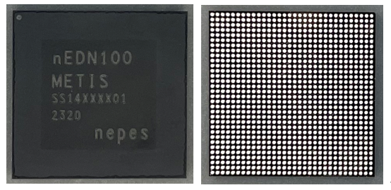
▲Intelligent semiconductor ‘Metis’ for edge computing equipped with deep learning acceleration IP
Nepes (CEO Byeong-gu Lee), a cutting-edge semiconductor back-end process foundry company, announced on the 27th that it had succeeded in developing ‘METIS’, an intelligent semiconductor for edge computing.
In April 2021, Nepes Artificial Intelligence Research Institute was selected as the 'Development of Intelligent Edge Computing Semiconductor for Lightening Manufacturing Inspection Equipment' project in the 'Artificial Intelligence Semiconductor Application Technology Development Project' hosted by the Institute for Information and Communication Planning and Evaluation (IITP) under the Ministry of Science and ICT in April 2021. was selected as the host company and conducted research through an industry-academia-research consortium with the Korea Institute of Electronic Technology and Hanyang University.
The researchers developed a deep learning model for ultra-lightweight/ultra-precision manufacturing inspection equipment based on an automatic lightweight software framework with the research goal of ultra-lightweight/miniaturization, low-power consumption, and low-cost of existing server- or PC-based manufacturing inspection systems. Furthermore, using this, a deep learning acceleration IP optimized for data reuse and parallel computing processing was completed and installed on Metis.
As a result, Nepes has developed a neural network-based deep learning defect detection algorithm that can reorganize the existing server-centered AI system into a terminal-centered one, and has secured a low-power SoC platform technology that reflects this. Through technological advancement, it has been able to increase productivity and efficiency at the manufacturing site. We hope to be able to contribute.
In addition, Metis applied cx-BGA (Ball Grid Array) of nePACTM, Nepes' cutting-edge 2.5D & 3D package platform. nePACTM is a next-generation cutting-edge package technology that implements multi-layer and fine RDL wiring based on fan-out technology and flip chip bonding technology, and is suitable for highly integrated, high-performance chips such as artificial intelligence semiconductors.
Yeonsook Park, head of Nepes Artificial Intelligence Research Center, said, “Through this research, we will solve network traffic issues in existing cloud server-type systems and secure intelligent processor technology that can detect defects at the edge, thereby developing various deep learning-related applications needed throughout the industry. “We have been able to accelerate it,” he said.
Meanwhile, Nepes is carrying out national projects to develop core packaging technologies for system semiconductors and AI semiconductors, such as 'Development of chiplet heterogeneous integration ultra-high-performance artificial intelligence semiconductors' with a total project cost of KRW 44 billion hosted by the Ministry of Science and ICT, as well as AI semiconductors specialized for on-device. We are working to secure original technology.