Panel Remarks at Semiconductor Advanced Packaging Expert Forum… Emphasizes 300mm Testbed and Joint FAB
Nepes, a system semiconductor company, has presented strategic directions for building a domestic advanced packaging industry ecosystem. At the Semiconductor Advanced Packaging Expert Forum held at the Lotte Hotel in Seoul on the 23rd, Nepes Vice President Kim Jong-heon emphasized, "We must turn our technological latecomer status into an advantage. We desperately need a government-led open innovation platform that can bring together the technologies and capabilities of the entire industry."
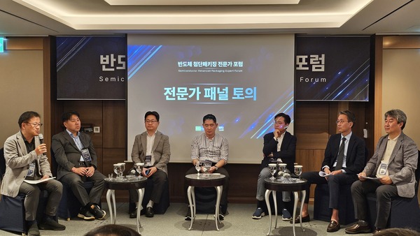
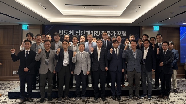
Hosted by the National Nanotechnology Foundation (NNFC) and attended by approximately 30 experts from industry, academia, research, and government, the forum was designed to explore ways to secure advanced packaging infrastructure in response to the proliferation of AI and HPC. As the domestic and international semiconductor ecosystem shifts its focus from front-end processes to back-end technologies, the strategic importance of packaging technology has been highlighted.
The discussion, attended by Vice President Kim, Hyundai Motor Securities, Amkor Korea, the Korea Electronics Technology Institute, and the Korea Fabless Industry Association, involved in-depth discussions on advanced packaging technology strategies, global infrastructure benchmarking, and the establishment of a public-private partnership model.
Meanwhile, the government, under the leadership of the Ministry of Science and ICT, is promoting the "Semiconductor Advanced Packaging Infrastructure Construction Support Project," which aims to secure advanced packaging equipment and processes based on 300mm wafers by 2029 and operate them as an open platform.