Nepes,
led by CEO Byung-Koo Lee, participated in the inaugural '2023 Advanced
Semiconductor Packaging Show’ upon invitation from Samsung Electronics' AVP
(Advanced PKG) business team.
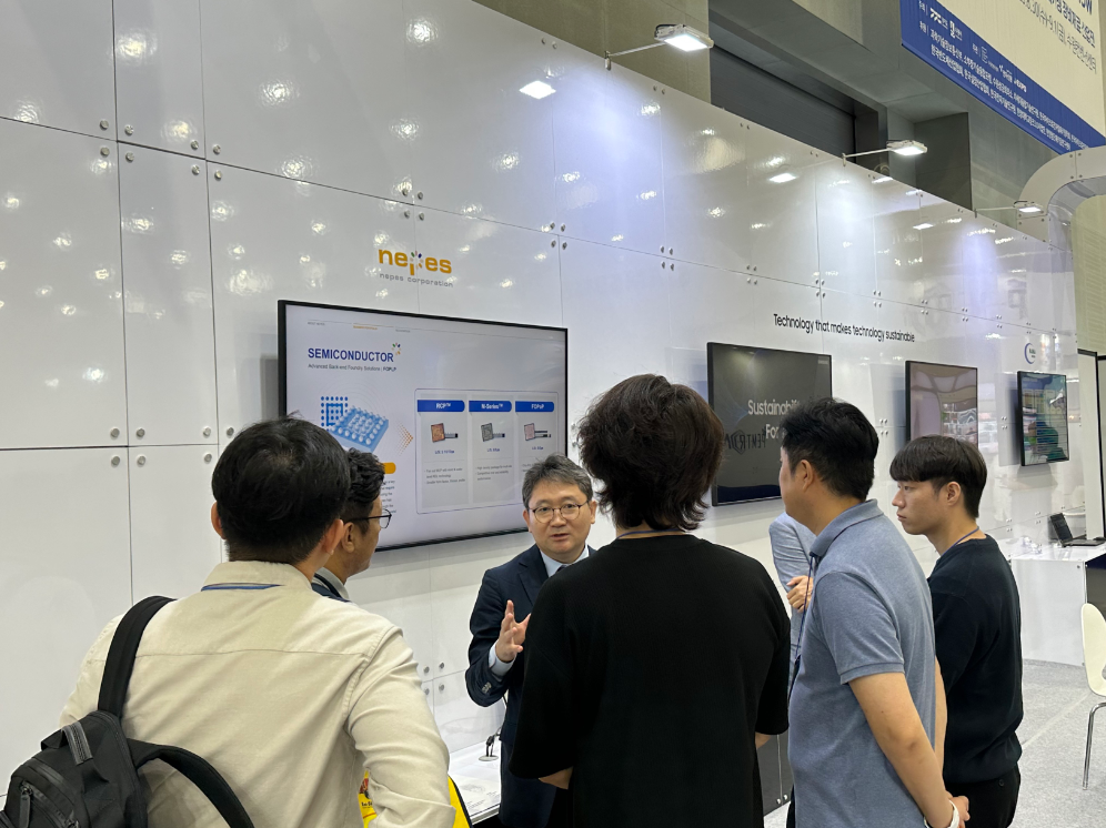
▲ Kang In-soo, Executive Director, explaining Nepes' advanced
packaging technology to the visitors. (Photo= Nepes)
With
the advanced semiconductor process facing significant costs and technical
challenges, packaging technology to enhance chip performance is gaining
attention. Last year, Samsung established an AVP (AdVanced Packaging) team to
nurture advanced packaging and strengthen collaboration with technically
capable partners. Having provided advanced packaging services since 2000,
Nepes, as a core partner of Samsung, was invited to this exhibition, where they
introduced their expertise through high-quality WLP processes, FOPLP, and the
ultra-compact SiP, nePAC, captivating attendees' attention.
Co-hosted
by Suwon City and Gyeonggi Province, the '2023 Next-Generation Semiconductor
Packaging Equipment and Materials Industry Exhibition', the first post-process
specialized semiconductor exhibition in Korea, opened on the 30th and will run
for three days at the Gyeonggi Suwon Convention Center, ending today(9/1).