- Stable yield achievement of 600mm FOPLP Fab at
Cheongan Campus ... Mass production ramp-up
- The world's first large-panel packaging process
enabling significant productivity improvement and more accessibility to
'advanced technology'
Nepes Laweh announced that it will more than double
its capacity next year as it begins mass production of FOPLP, the
next-generation packaging process.
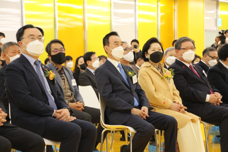
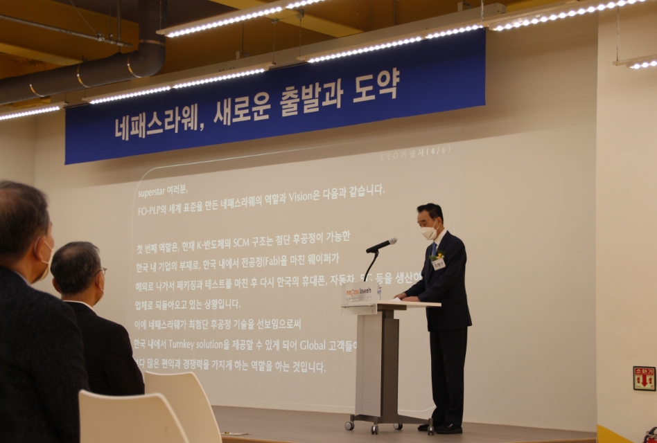
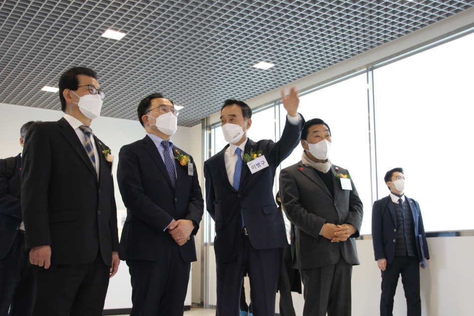
Nepes Laweh held the completion ceremony of the
Cheongan Campus PLP fab on December 7th with the presence of Minister of Trade,
Industry and Energy, Governor of Chungcheongbuk-do, and representatives from
customers and partners.
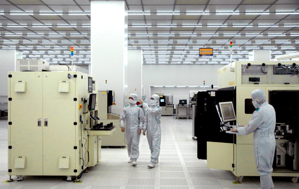
The company announced that the FOPLP manufacture line
completed customer certification in the third quarter and achieved a stable
yield and started full-scale mass production and plans to more than double its
capacity next year aligned with strong customer demand.
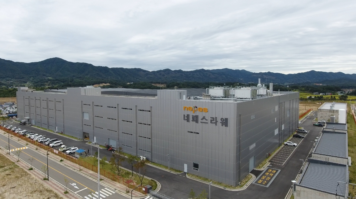
The PLP Fab, where the completion ceremony was
held, was the first fab built on the 186,000㎡ Cheongan Campus site which is the size
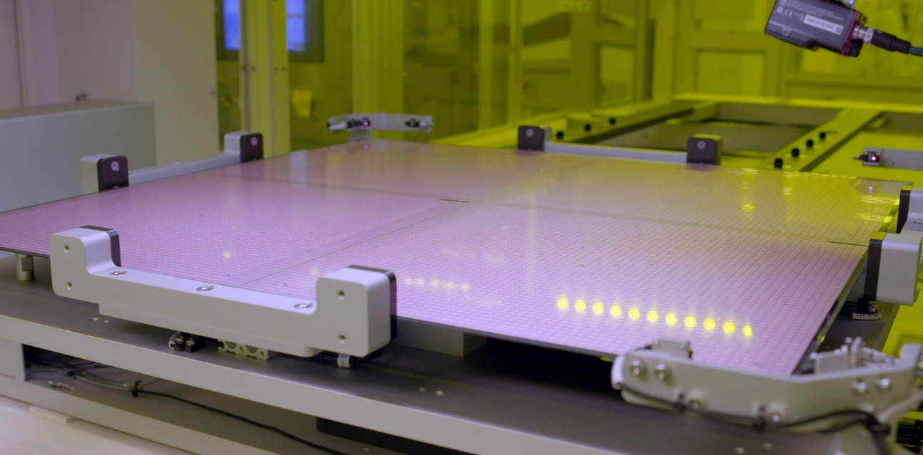
of 25 soccer fields: with a total building area of 34,000㎡. The fab can produce up to 96,000 panels per year based on 600mm
PLP.
Based on this next-generation packaging line, nepes
would receive a favorable evaluation about her ability to provide high-density
packaging solutions required for Non-memory semiconductors for each
application, such as smartphones, automobiles, and IoT, aligned with customer
needs.
"FOPLP is the best packaging solution for
high-end semiconductors as a result of long cooperation with global partners
such as materials, parts, and equipment," said Chilhee Chung, Chairman of
Nepes and GM of Semiconductor Business
According to the industry, nepes laweh's FOPLP is a
large square panel with a size of 600mm by 600mm, and it is analyzed that
productivity has greatly improved compared to the 300mm round FOWLP. In
particular, the fan-out technology applied to Nepes Laweh’s FOPLP has been
proven to have high stability compared to existing technologies.
As demand increases mainly from advanced
semiconductor manufacturers in the future, its market share is expected to
significantly increase in the overall packaging market.
About Nepes Laweh
Nepes Laweh is leading company in the system semiconductor
industry with advanced fan-out packaging solution. In the era of the 4th
industrial revolution, when semiconductors are refined and advanced, such as
5G, self-driving cars, and smartphones, we are presenting new standards for
fan-out packages based on nPLP™ technology using 600mm large square panels.