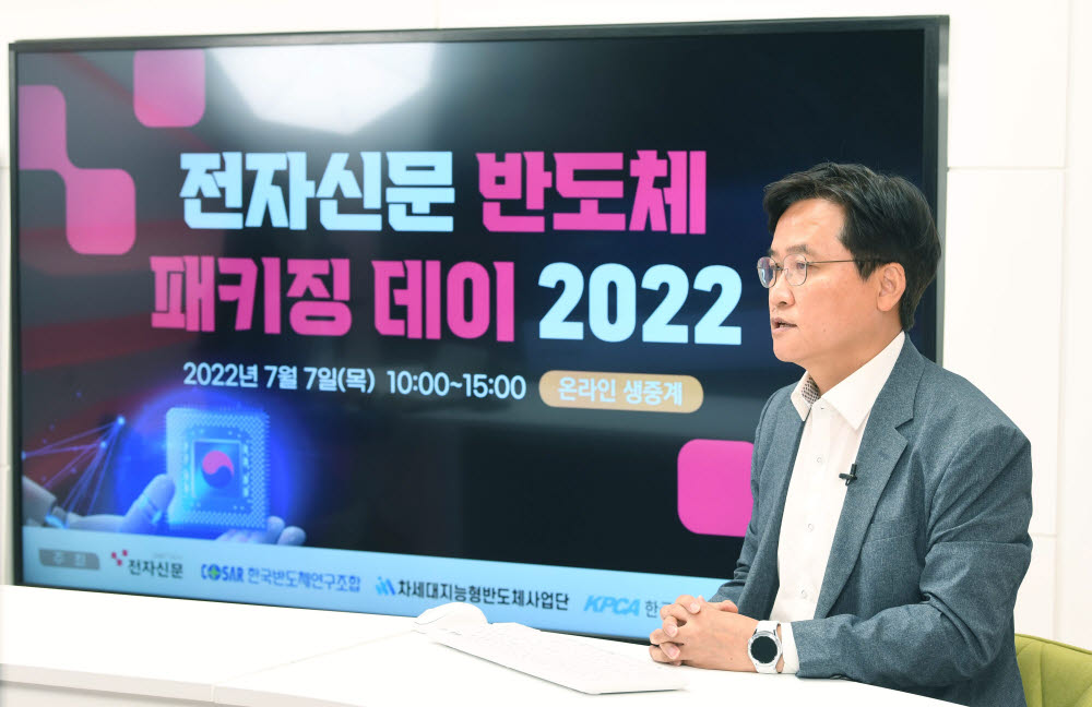
[Semiconductor Packaging Day 2022] Nepes expands the application area of FO-PLP.
Nepes will expand its mass-production products using fan-out-panel level packages (FO-PLP), one of the most advanced packaging technologies.
Following the Power Management Integrated Circuit (PMIC), market will be expanded with codec chips and application processors (AP).
It will also respond to demand for next-generation packing markets such as system-inpackage (SiP) and 2.5 and 3D utilizes Nepes' advanced fan-out (FO) technology.
During the “Semiconductor Packaging Day 2022”, Kim Jong-heon, Nepes' Corporate CTO of Semiconductor Business (Executive Vice President), said in
“We are increasing applications such as codecs after last year’s mass-production of the world’s first PMIC with FO-PLP",
“We will mass-produce AP, and APU, which combines AP and GPU, as FO-PLP in the future.,” he added
FO-PLP is a technique that packages square panels rather than round warfers.
Nepes has a mass production technology of 600mm panels in width and height.
It is considered a next-generation technology that can increase production speed by more than five times compared to packaging on a typical 12-inch wafer.
Nepes have been supplying PMIC of global semiconductor companies with FO-PLP since the fourth quarter of last year.
For the first time in the industry, Nepes has invested hundreds of billions won in building FO-PLP mass production facilities.
Nepes have also begun the mass production of codec chips as well as PMIC.
It is known that other chips, such as AP, are currently being discussed with customers for the mass production of FO-PLP. The specific customer company is not disclosed.
Vice President Kim said, “In addition to single-chip FO-PLP, there are many more products when considering the packaging of two or more chips. The expansion of the FO-PLP market is as expected.
Nepes will also be launching its next-generation packaging market. Typical examples are 2.5D and 3D packaging, and 3D package-on-package (PoP) technology.
PoP is a technology that stacked packages which function differently from packages. Nepes developed an ultra-thin PoP with minimal heat and reduced package thickness and passed the technical qualification.
Vice President Kim explained that the packaging thickness can be reduced up to 26% compared to his competitors.
SiP without substrates is also a field that Nepes focuses on. It introduced its first mass-production product earlier this year with SiP that utilizes Nepes' own RDL technologies.
It reduces the size to one-third of the existing package and shortens the signal transmission distance by 30%. Nepes is also developing a 3D stacking technology that vertically stacked semiconductors.
Nepes' entry into the next-generation packaging market is based on its excellent fan-out technology.
Fan-out is a technology that increases the number of I/Os by placing semiconductor input and output terminals (I/O) outside of the chip and can exchange more signals.
Vice President Kim said, “Nepes possesses a wide range of advanced packaging technologies to provide packaging solutions that are ahead of their time.”he also said
“We plan to play a role as a high-tech back-end foundry rather than a simple back-end process.”

