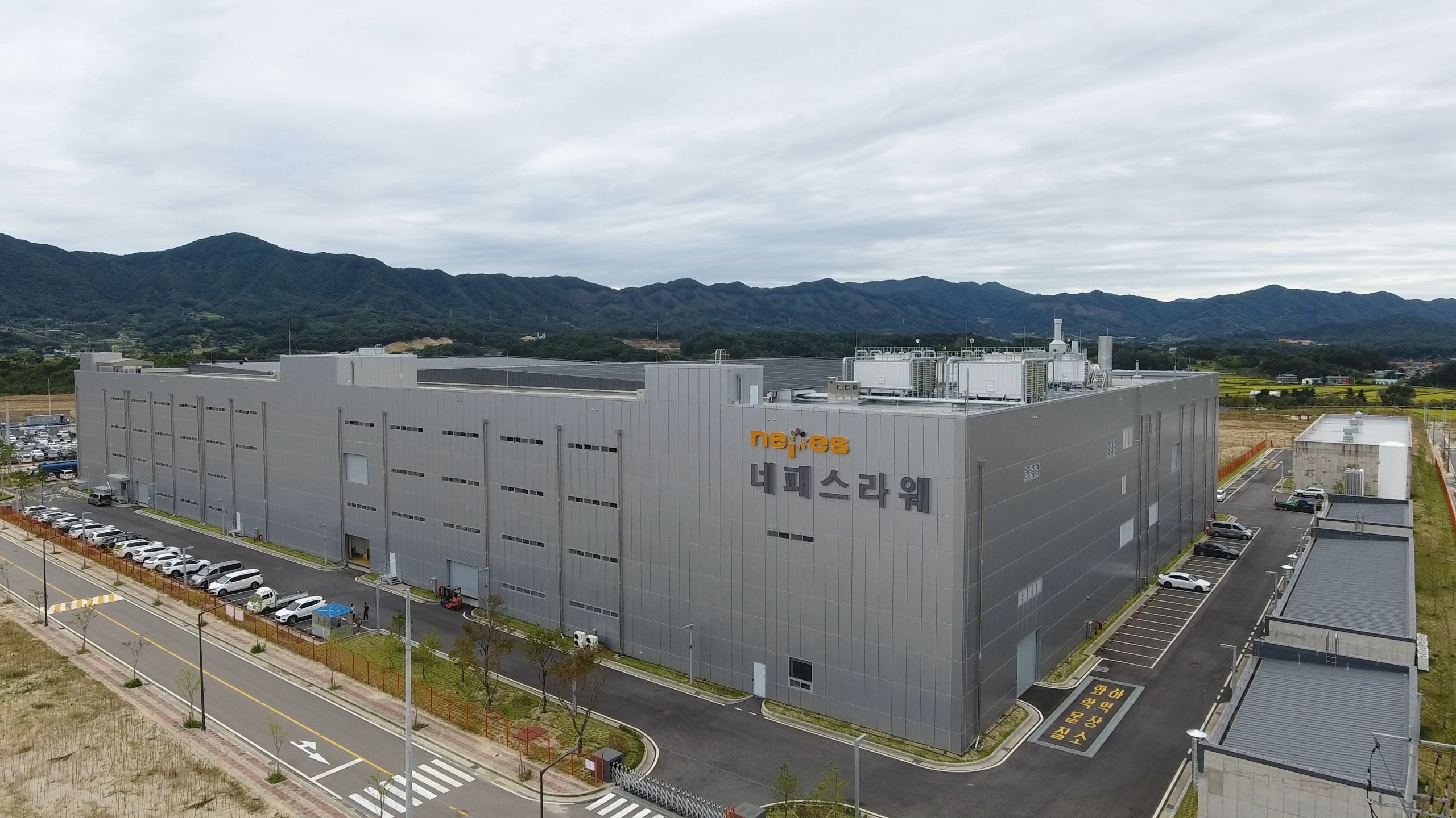
Nepes Laweh corporation
announced the successful production qualification and ramp-up of the world’s first 600mm x 600mm large panel manufacturing line using Deca’s M-Series™ fan-out technologies.
Nepes Laweh held the completion ceremony of
the Cheongan Campus PLP Line on December 7th with the presence of Minister of
Trade, Industry and Energy, Governor of Chungcheongbuk-do, and representatives
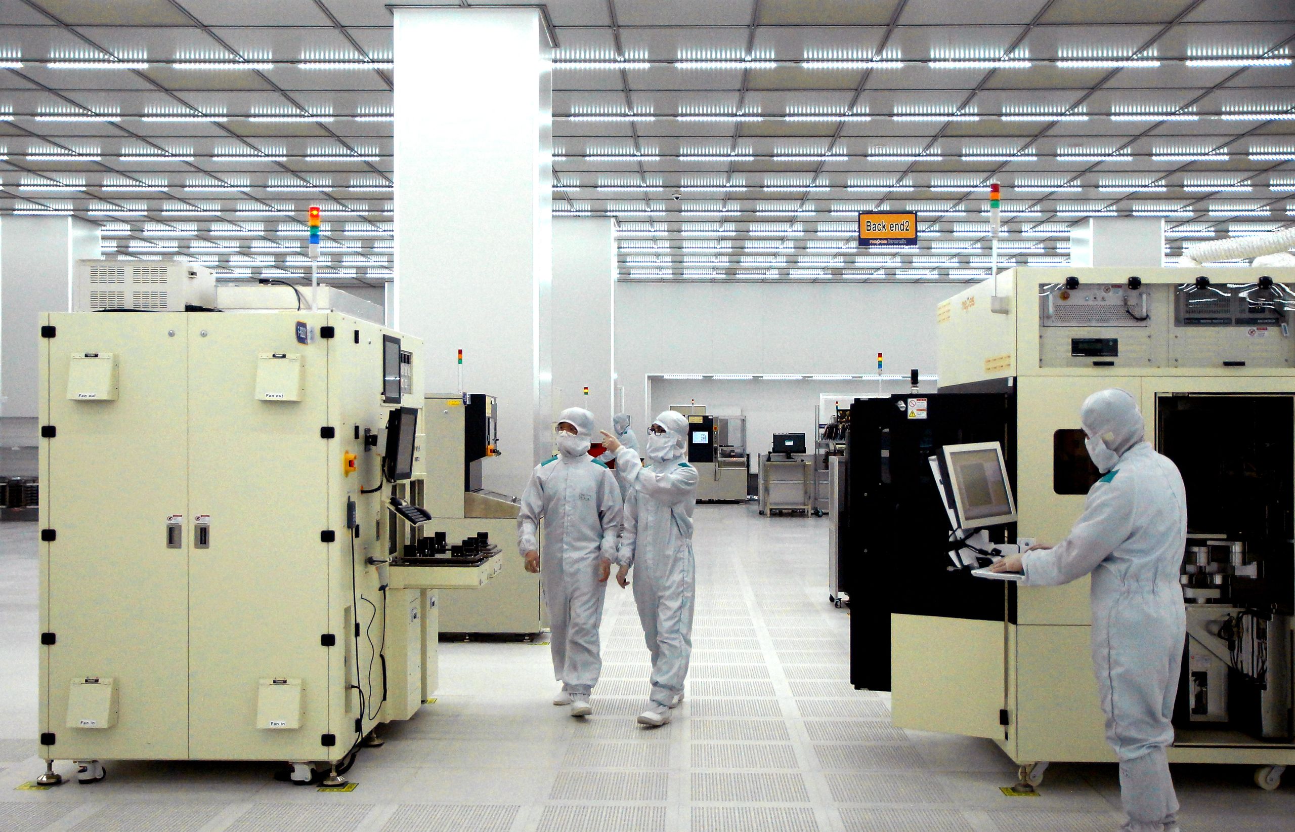
of customers and partners. The company announced that the FOPLP line completed
customer certification in the third quarter and secured a stable yield and
entered full-scale mass production.
The PLP fab, which held the completion
ceremony this time, was the first fab built on the 186,000㎡ Cheongan Campus site with 25 soccer fields, and was a total
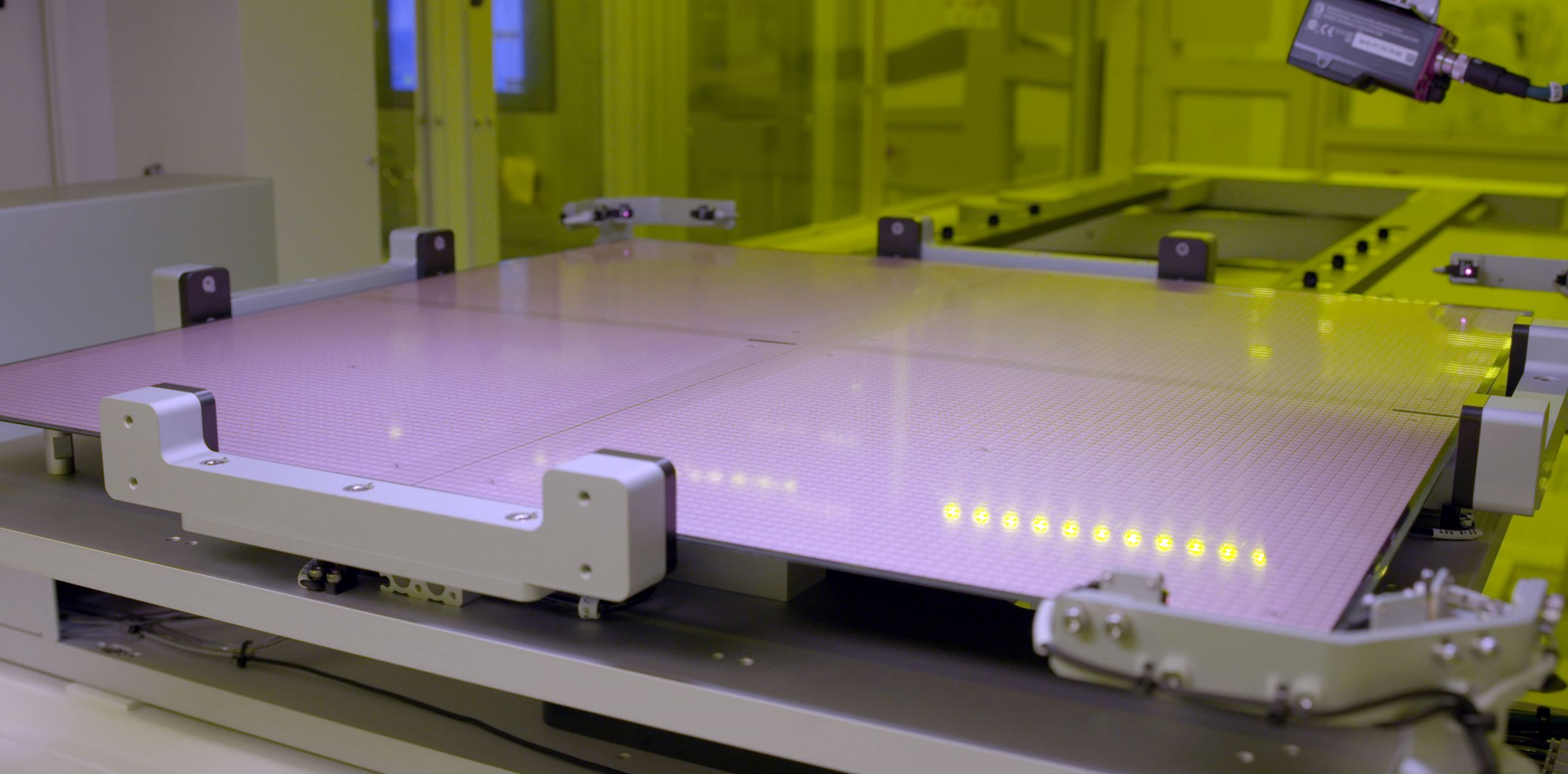
building area of 34,000㎡. This is a level that can
produce up to 96,000 panels per year based on 600mm PLP. Based on this
next-generation manufacturing line, Nepes is evaluated to be able to provide
high-density packaging solutions required for advanced system semiconductors
for each application, such as smartphones, automobiles, and IoT, according to
customer needs.
"FOPLP is the best packaging solution
for high-end semiconductors as a result of long cooperation with global
partners such as materials, parts, and equipment," said Chilhee Chung,
Chairman of Nepes and GM of Semiconductor Business
“We’re pleased to be working
with nepes to bring the industry’s largest format 600mm
square panel to volume production” commented Tim Olson,
CEO of Deca. “With initial production focused on single
and multi-die packages for leading Smartphone producers, the future is
heterogenous integration of chiplets using Deca’s Gen 2
technology. A recent customer application with 10 embedded chiplets was
designed into a 36mm x 36mm package. Such a large device is limited to
73% maximum utilization on 300mm round format due to edge losses. On
600mm, the utilization jumps to 92% delivering greater than 25% cost reduction
on area utilization alone.”
About Nepes Laweh
www.nepes.co.kr
Nepes Laweh is leading
company in the system semiconductor industry with advanced fan-out packaging
solution. In the era of the 4th industrial revolution, when semiconductors are
refined and advanced, such as 5G, self-driving cars, and smartphones, we are
presenting new standards for fan-out packages based on nPLP™ technology using 600mm large square panels.
About Deca Technologies
www.ThinkDeca.com
Deca is a leading provider of advanced packaging
technology to the semiconductor industry with M-Series™ fan-out and
Adaptive Patterning® real-time design-during-manufacturing. A
growing list of industry leaders have completed technology transfer and license
agreements for access to Deca’s proven structures, processes, materials,
equipment, design systems and know-how.
Starting with the highest quality and reliability in Gen 1 aimed at
Smartphone applications to the growth of Gen 2 for chiplets and heterogeneous
integration, Deca’s technologies are emerging as key industry standards for the
future.