

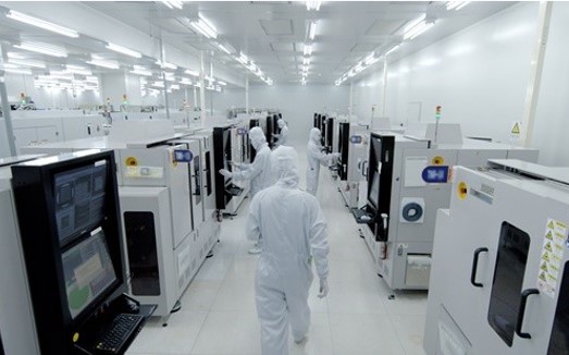
![[Report] Nepes, a Key Material, Part, and Equipment Company, Returns to Korea…Fitting Up the Supply 이미지1](https://www.nepes.co.kr/data/bbsData/17560882629.jpg)

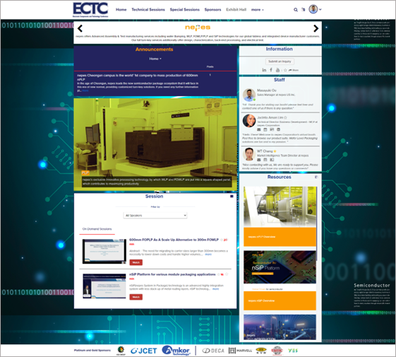
![[Semiconductor Packaging Day 2022] Nepes expands the application area of FO-PLP. - ETnews 이미지1](https://www.nepes.co.kr/data/bbsData/16576096149.jpeg)

-
 NEWS
NEWS
-
 Nepes Selected as a Government-Organized "Innovation Premier 1000" Company
The "Innovation Premier 1000" program, jointly operated by 13 government ministries, including the Financial Services Commission, aims to identify small and medium-sized enterprises (SMEs) with innovative potential and growth potential and provide them with tailored financial and non-financial support through collaboration with policy finance institutions. A total of 509 companies were selected through collaboration between relevant ministries and policy finance institutions, and Nepes was included in the list under the Ministry of Trade, Industry and Energy's Semiconductor and Display Division. Nepes received excellent recognition for its advanced packaging technology, AI semiconductor capabilities, and its expansion of its global customer base. Meanwhile, the Innovation Premier Program plans to expand its support to 1,000 companies annually starting in 2026, and the companies selected in the first round will receive intensive policy support until the end of 2026.
2025-05-20 -
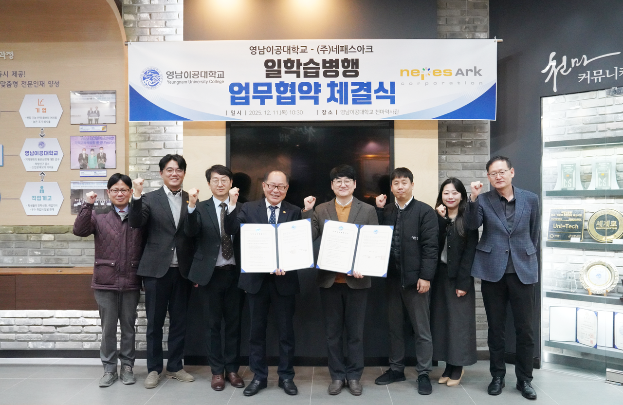
 Nepes - Inha University Manufacturing Innovation Graduate School Semiconductor Professional Training
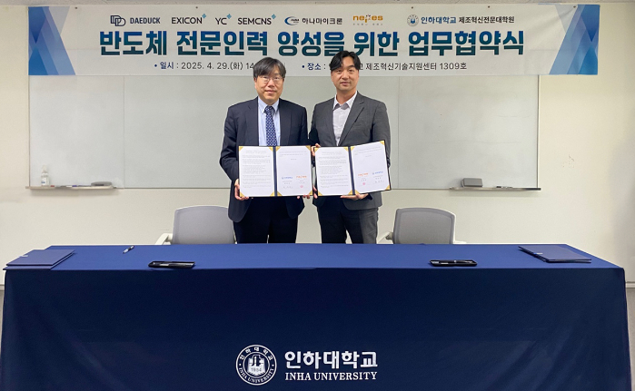
On April 29, Nepes signed an agreement with Inha University’s Graduate School of Manufacturing Innovation for cooperation in fostering semiconductor professionals.The signing ceremony was attended by seven people from the semiconductor industry, including Nepes, Hana Micron, SEMCNS, YC, EXICON, DAEDUCK. With this business agreement, Inha University has decided to foster specialized personnel in the semiconductor process intelligence convergence master’s course with government support until 2031 in order to systematically cooperate in fostering personnel, including the full cycle of semiconductor industry intelligence, including fostering new personnel, fostering incumbent R&D personnel, and strengthening practical capabilities, fostering packaging specialists, and specializing personnel in utilizing semiconductor infrastructure.
2025-05-02 -
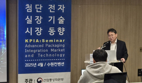 Nepes, Targeting the Popular Edge Computing Market with Advanced Packaging Technology
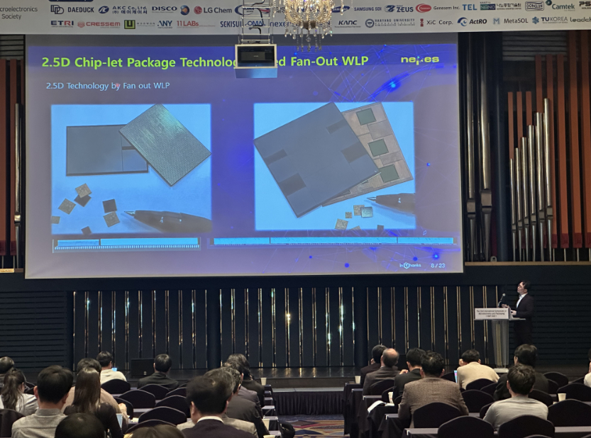
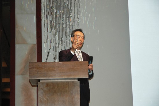
Nepes, a semiconductor post-processing (OSAT) specialist, is targeting the popular edge computing market with advanced packaging technology based on the fan-out (FO) process. It plans to target the 2.5D packaging and chiplet markets based on technologies such as RDL (re-wiring) interposers and silicon bridges. Kang In-soo, head of Nepes Semiconductor Research Institute (executive director), explained at the ‘Advanced Electronic Assembly Technology and Market Trend Seminar’ held at the Suwon Convention Center on the 2nd, “We are talking about on-device (edge) AI now, but in reality, it seems that the algorithms suitable for it have not yet transitioned to edge computing.” He added, “The inference AI market is expected to grow 10 times larger than the learning market in the future, which means that the AI market that we can enjoy has not yet arrived.” He added, “I think the true AI era will come when we transition to popular edge computing, and we need to prepare for that era.”View original article = 네패스, 첨단 패키징 기술로 보급형 엣지 컴퓨팅 시장 공략- 시사저널e
2025-04-10 -
 Cheongju City -Nepes, Signing Investment Agreement for Expansion of High-Performance Advanced Semico
Cheongju City announced on the 28th that it signed an investment agreement worth 160 billion won with Chungcheongbuk-do and Nepes, a system semiconductor advanced packaging specialist. The agreement was signed on the 27th.Nepes is a mid-sized company with global competitiveness in the system semiconductor advanced packaging sector. Through this agreement, it plans to invest in expanding production facilities at Ochang Plant 2 in Ochang-eup to respond to the increasing demand for high-performance AI semiconductors.With the expansion, Nepes is expected to establish itself as a global supplier of semiconductor packaging for AI data centers and chiplet (2.5D, 3D)* packaging.*Chiplet: A technology that designs and manufactures a single chip by dividing it into multiple small modular chips. Mainly used to integrate AI semiconductors and HBM (high bandwidth memory) into a single package.Cheongju City will actively support companies to carry out their business stably, and Nepes will actively participate in the development of the local economy by giving priority to local residents for new hires, participating in local construction companies, and purchasing local materials.A city official said, “Through this investment by Nepes, Cheongju’s status as a center for the advanced semiconductor industry will be further solidified,” and “We will not spare any support to ensure that the business is carried out smoothly.”Lee Byeong-gu, CEO of Nepes, said, “We will actively respond to the increasing demand for semiconductors for AI, such as data centers, autonomous driving, and humanoid robots, build a K-semiconductor cluster ecosystem, and achieve greater growth in the global semiconductor market.” He added, “We will also contribute to the revitalization of the local economy by coexisting with the local community.”청주시-㈜네패스, 1600억 ‘투자 협약’…AI 반도체 생산시설 확장 | Save Internet 뉴데일리
2025-03-31 -
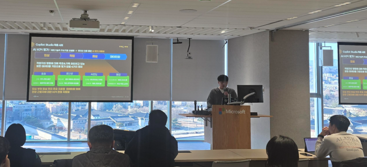 Nepes, strengthens corporate competitiveness with AI innovation strategy
On December 17, Nepes presented the application cases and future direction of Copilot Studio at a seminar held at Microsoft Korea. Part Manager Kwon Hyo-jin (CIO HQ Information System Team), who was in charge of the presentation, shared the company's case of building large-scale data processing and infrastructure through AI Build-Up, securing various types of large-scale data to create a flexible work environment, and said that it is using this to help with quick decision-making by utilizing AI training and personal AI assistants.Nepes introduced M365 Copilot in August and maximized work efficiency by utilizing generative AI functions in various M365 products such as Teams, Outlook, Word, Excel, and PowerPoint. Starting next year, it plans to introduce Copilot plugin and Action Copilot to launch system automatic control AI service. In addition, Nepes introduced HRSM service through HR innovation project to improve the quality of HR service and visualize and improve the efficiency of HR work progress. It improved the evaluation method by establishing an AI KPI evaluation system through data-based evaluation and automation, and increased real-time inquiry response and HR work efficiency by introducing AI Copilot for year-end settlement.In the future, Nepes plans to introduce PBL (Project Based Learning) to secure AI manufacturing competitiveness and operate the Copilot power user training program so that all employees can utilize the AI secretary. Part Manager Kwon emphasized that Nepes will continue to pursue AI innovation and supply and operate a stable system for global business expansion.
2024-12-26 -
![[DIC2024] Nepes Increases Production and Reduces Costs for FO Packaging 썸네일](https://www.nepes.co.kr/data/bbsData/17461609729.jpg) [DIC2024] Nepes Increases Production and Reduces Costs for FO Packaging
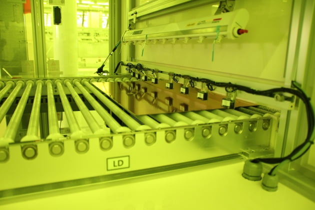
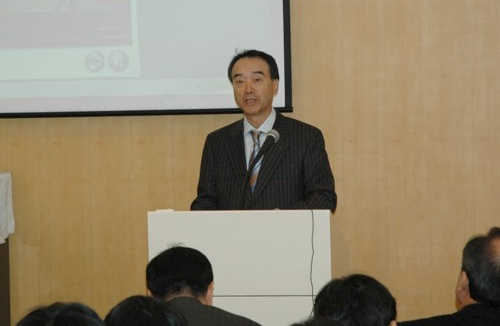
[DIC2024] Nepes Increases Production and Reduces Costs for FO PackagingJong Heon Kim, head of Nepes' Technology Development Division, gives a presentation on 'Trends and Role of Advanced Packaging Technology in High Performance Products' at the '2nd DigitalDaily Industry Conference (DIC) 2024', held from 1:00 p.m. on November 21st at the Yeouido FKI Tower Conference Center Diamond Hall in Seoul, Korea .[DigitalDaily reporter Kim Moon-ki] “Our continued efforts in packaging for the production of semiconductors in the AI era aim to increase production capacity. Nepes strives to bring not only productivity but also price competitiveness through fan-out (FO) packaging technology to silicon interposer. We will provide multiple services on a two-track basis, including technologies that cover 2.5D packaging and hold multiple chips in one package.”Jong Heon Kim spoke about Nepes' competitiveness on the topic of 'Trends and Role of Advanced Packaging Technology in High Performance Products'. “The current semiconductor market resembles a war more than a strategy. As the market gradually localizes, we must focus on our strengths,” Kim said, adding that ”the same is true for the advanced packaging field.”The pressure to follow Moore's Law is on, he notes. The curve of Moore's Law, which requires a doubling of scale every two years, has been bent. It costs around $500 million to design and test an existing chip and $30-40 million to produce a single wafer. Difficulties in manufacturing and prolonged periods of development, along with the high cost are proving to be a challenge. “Packaging is the answer to physical limitations, manufacturing difficulties, and cost reduction,” said Kim. ”If there is a best practice in the construction of existing SoCs, we should follow it. Currently, chiplets are on the rise, as they can be divided by functions, in which simple processes and difficult processes are separated and put back together in the later stage of production."Kim, however, points out that while silicon intensifiers offer high performance and efficiency in 2.5D packaging, they can be costly. An alternative is fan-out (FO) and wafer-level package (WLP) technology, which Nepes focuses on. This technology involves packaging chips on a wafer-by-wafer basis. It is advantageous for cost reduction as it eliminates the need for printed circuit boards (PCBs) and reduces the number of processes.<source=nepes corp.><source=nepes corp.>Kim also emphasized the need to foster the entire cycle of production from Front-end process to Back-end process.“Even if the process is broken down into chiplets and put back together again, chip design and packaging must work together organically," he said. “In other words, it is important to build an ecosystem where the front and back are connected. In the end, the packaging and the chip must be designed together,” he said.“It is said that Korea's competitiveness requires reviewing packaging from its beginning stage. We believe that there is potential and possibility to foster a whole ecosystem of AI semiconductors because we have AI data, foundries, and data-based platform companies," he said, adding, "Korea is also in dire need of technology collaboration." [Source = DigitalDaily [DIC2024] 김종헌 네패스 “FO 패키징 ‘생산증가 원가절감’…韓 디자인-패키징 공급망 강화해야” - 디지털데일리]
2024-11-25 -
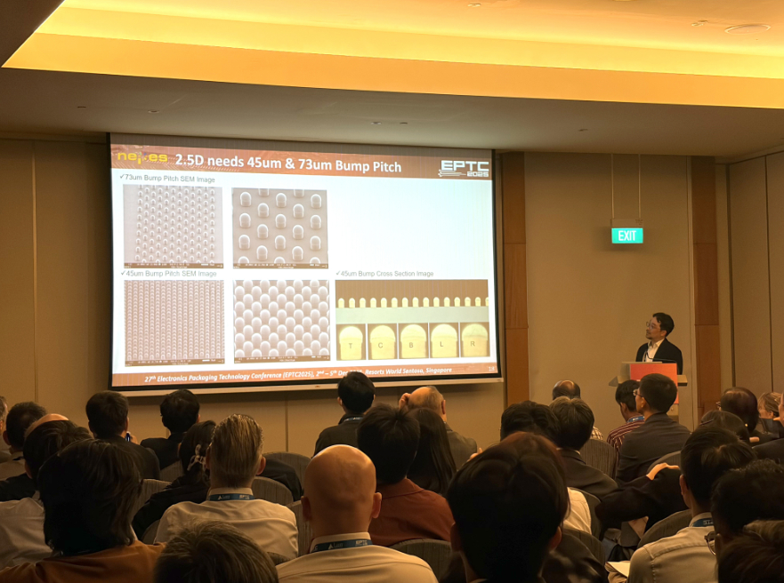
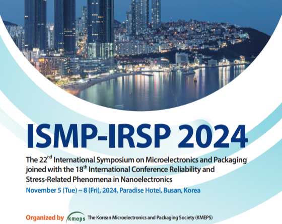 Nepes Participates in IMSP 2024
Nepes participates in the International Symposium on Microelectronics and Packaging (ISMP), an international conference dedicated to the latest trends in semiconductor packaging technology. The 22nd ISMP, organized by the Korea Society of Microelectronics and Packaging, is held on November 6-8 at the Paradise Hotel in Busan, and is co-hosted with the 18th International Conference Reliability and Stress-Related Phenomena in Nanoelectronics(IRSP).On November 6-7, Nepes will introduce its core technologies, including chiplet and 2.3D technologies, at Lobby Booth 2. On November 6 at 3:50 p.m., Nepes Semiconductor Research Center's Advanced Technology Part Leader Lee Jung Won will present on the topic of “Chip-let Heterogeneous Integration Packaging Based on Fan-out RDL Interposer Technology”.
2024-11-06 -
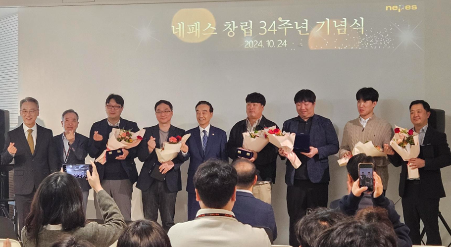 Nepes Holds 34th Founding Anniversary Celebration
Nepes celebrated its 34th founding anniversary on October 24th. Nepes held the ceremony from 8:30 a.m. with a worship service of thanksgiving, a commemorative video screening, a message from the CEO, and a special music class. All employees participated online and offline to share in the celebration. Afterwards, Nepes held various commemorative events such as long-term service awards for each campus, autumn hikes, and a gratitude bazaar.“For 34 years, our company has been able to grow steadfastly in the face of numerous challenges. This is thanks to our shared dreams and visions, and your dedication to doing your best in your respective positions,” said Byung Koo Lee, CEO of the company. “We have the DNA to turn turbulent external environments into opportunities for revitalization,” he said, encouraging employees that "Here at Nepes, we are the superstars who strive to be the ’The First of Yesterday and the Best of Tomorrow'".Lee also said, “To make another 34 years of expectation and excitement into an opportunity to rebound, we must first create synergy by inspiring a sense of mission in what we do. Second, we must fulfill our business plan goals with a sense of responsibility and vocation. Third, we will create an energetic and exciting work environment”.
2024-10-25 -
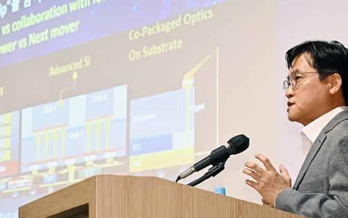
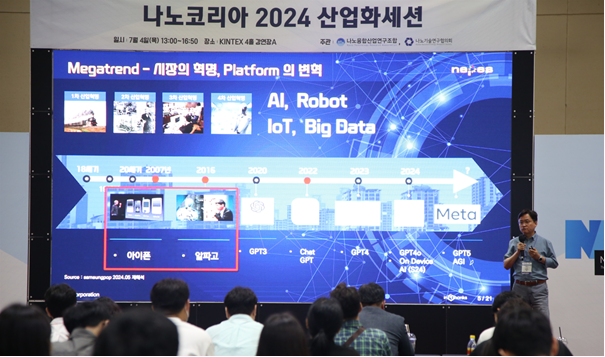 Nepes Kim Jong Heon Lectured advanced semiconductor packaging at 'Nano Korea 2024 Industrialization
▲Kim Jong-heon, Vice President, Lecture at the 2024 Industrialization Session of Nano KoreaNepes gave a lecture on advanced semiconductor packaging technology at 'Nano Korea 2024 Industrialization Session' held at KINTEX 1st exhibition hall in Goyang City on the 4th.Kim Jong-heon, vice president of Nepes CTO, said, "The advanced packaging technology in AI era; Chiplet and Integration ', introduced chiplet and heterogeneous packaging technology, a cutting-edge semiconductor packaging trend.Nano Korea is one of the world's top three nanotechnology events, hosted by the Ministry of Trade, Industry and Energy and the Ministry of Science and ICT, and organized by the Nano Convergence Research Association and the Nanotechnology Research Council. Among them, the industrialization session is a program that domestic and foreign global companies announce in-depth about the direction of their nanotechnology commercialization, and invited nine speakers of next-generation semiconductor and display industries, including Nepes, Samsung Electronics and SK Hynix, to give lectures.Vice President Kim Jong-heon said, "The development of Gen AI is accelerating changes in many fields such as life and industry," and explained, "In the packaging field as well as the entire semiconductor process, AI semiconductor-oriented bumping, 2.5D, and chiplet technologies continue to develop, and Nepes also has and develops related technologies and is pushing for commercialization."He added, "In addition to packaging technology, heat dissipation performance, which is closely related to power consumption, is also becoming important." He emphasized the importance of developing innovative materials along with package structure design.Meanwhile, Nano Korea is a high-tech exhibition that can confirm the commercialization status of nanotechnology and roadmap of famous domestic and foreign companies. 400 companies from 40 countries participated and 12,000 people visited.
2024-07-08 -
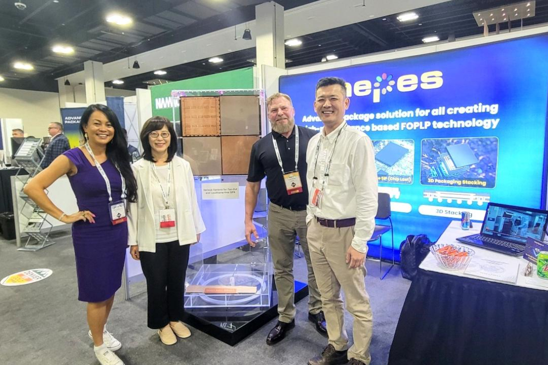 Nepes Participates in the 2024 ECTC
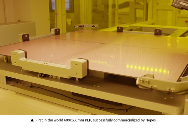
Nepes participated in the 2024 Electronic Components and Technology Conference (ECTC) in Denver, Colorado, USA from May 28 to 31 (local time) to showcase advanced semiconductor packaging technology.Celebrating its 74th anniversary this year, the 2024 ECTC is an international event hosted by the IEEE-affiliated Electronics Packaging Society and boasts the world's largest electronic component technology society.Nepes presented a 600mm FOPLP solution and a chipset packaging based on a fan-out RDL interposer at the event.On the next day of the event, the technical program participated in the announcement of advanced packaging technology with Samsung Electronics and SK Hynix as Korean companies.Nepes introduced the excellence of FOPLP as a replacement for the traditional package QFN, titled '600mm x 600mm Fan-Out Panel Level Package (FOPLP) as an Alternative to Lead-Frame-Free Quad Flat No Lead (QFN) Package'.In the Interactive Presentations session held on the same day, I also presented my thesis on 'Single and Multi NPU Chiplet Heterogeneous Integration Packaging Based on Fan-Out RDL Interposer with Silicon Bridge Technology'.
2024-06-03 -
 Nepes pushes for commercialization of AI semiconductor packaging
Nepes has developed next-generation packaging PoP (Package on Package) technology for artificial intelligence (AI) and advanced semiconductor, and is working with domestic and foreign chip manufacturers to commercialize it.Recently, as the AI package market has been struggling with the global supply chain due to the oligopoly of Taiwanese companies, Nepes has developed and commercialized PoP technology, which is the base technology of 2.5D packaging *, utilizing its strengths, RDL technology.* 2.5D packaging: A technique for horizontally matching a semiconductor die on a wide substrate-shaped interposer, which is mainly used to integrate AI semiconductors and HBM (High Bandwidth Memory) into a single package.2.5D packaging, which is being developed by Nepes, has the advantage of price competitiveness and small form factor by implementing a rewiring (RDL) interposer using a fan-out process instead of an expensive silicon (Si) interposer.In particular, the developed PoP technology includes element technologies such as semiconductor device embedding technology, double-sided rewiring (RDL) technology, and Vertical Interconnection. It is a basic platform technology of advanced packaging that can expand its use to smartphone and automobile AP (Application Processor), wearable sensors, and AI semiconductors.Kim Jong-heon, chief executive officer of Nepes CTO, has been awarded "excellent performance by a global semiconductor company in Japan, a manufacturer of LiDAR sensors, which is a core technology for autonomous car, and is in the process of negotiating product applications. We are actively discussing commercialization. And based on the PoP technology developed this time, we will concentrate on 2.5D packaging technology for AI semiconductors and complete development with customers in the first half of 25 years and aim to mass-produce from the second half."Nepes is a strategic market that drives next-generation growth and aims to enter the commercialization of 2.5D and PoP technologies from the second half of 2025 by actively collaborating with AI server, automobile and edge computing product customers.press release inquiry : pr@nepes.co.kr
2024-05-20
Investor Relations
NEPES, GLOBAL TOP-TIER PARTNER