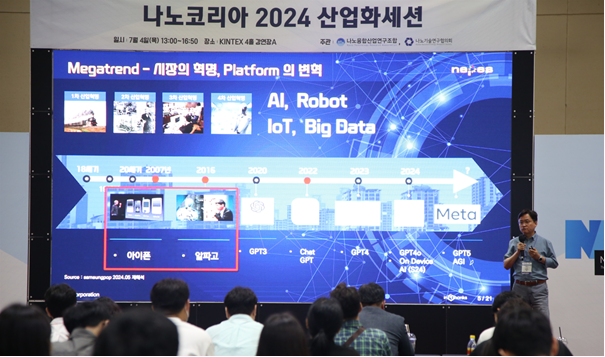
![[DIC2024] Nepes Increases Production and Reduces Costs for FO Packaging 이미지1](https://www.nepes.co.kr/data/bbsData/17461609729.jpg)

![[Semiconductor Packaging Day 2022] Nepes expands the application area of FO-PLP. - ETnews 이미지1](https://www.nepes.co.kr/data/bbsData/16576096149.jpeg)

-
 NEWS
NEWS
-
 nepes corporation expands IC packaging capabilities for the 3DIC era with advanced design flows from
Siemens Digital Industries Software today announced that South Korea-based nepes corporation, a global leader in Outsourced Semiconductor Assembly and Test (OSAT) services, has leveraged a range of industry-leading solutions from Siemens EDA to tackle the broad range of complex thermal, mechanical, and other IC packaging design challenges associated with developing advanced 3D IC packages.“nepes is committed to providing us with the most comprehensive portfolio of semiconductor packaging design and manufacturing services, to help us innovate and succeed in a market where high performance and compact form factors are critical.” said Brad Seo, vice president of SAPEON Korea’s R&D center. “By expanding nepes’ adoption and usage of Siemens’ EDA technologies for advanced packaging, we also can achieve the innovative technologies necessary to grow.”nepes has an established track record of providing customers with world-class packaging, testing, and semiconductor assembly services for clients throughout the global electronics industry. nepes also offers packaging design services including wafer level packaging, fan-out wafer level packages, and panel level packaging.Building on this foundation, nepes is now driving additional packaging innovation with a broad range of advanced technologies from Siemens EDA, including the Calibre® nmPlatform tool, HyperLynx™ software for electrical rule checking, Calibre® 3DSTACK software, as well as Siemens’ industry-leading Xpedition™ Substrate Integrator software and Xpedition™ Package Designer software. Together, these Siemens technologies helped nepes provide fast and reliable design services including 2.5D/3D-based chiplet designs for the company’s growing base of global IC customers....Read more : https://www.eejournal.com/industry_news/nepes-corporation-expands-ic-packaging-capabilities-for-the-3dic-era-with-advanced-design-flows-from-siemens/
2024-03-19 -
 Nepes enters the packaging market for AI
Due to the explosive growth of the generative artificial intelligence market such as Chat GPT, demand for advanced packaging of power semiconductors(PMIC) used in artificial intelligence systems is exploding.The product that Nepes has won this time and is starting to mass-produce is a power semiconductor for AI chipsets and a high-tech PMIC product that will expand into high-performance computing (HPC) and automobile markets in the future.Nepes has established a bridgehead for global HPC and automobile markets, starting with mass production of power semiconductors by Global Fabless (US). This new customer is a member of the value chain of AI products and is working with Nepes in a strategic partnership to prepare for explosive growth.Nepes is developing a number of its customers' products in its advanced packaging line, and it is confirmed that PMIC first shipped last year is installed in AI chipsets of GPUs, CPUs, consumers and IoT companies. Also, The product is expected to be adopted for ADAS for automobiles.In addition, the two companies are currently collaborating on a 12-inch project and plan to develop products using the 600mm PLP process in the future, diversifying their products and processes and securing competitive advantage in the market.As semiconductor manufacturing bases have recently accelerated their departure from China and Taiwan, strategic partnerships with global chipmakers and Nepes are expected to become more robust. Nepes will take this opportunity to increase its market share and continue to secure 2.5D / 3D capabilities, the next generation package for artificial intelligence.A Nepes official said, "Nepes currently has core customers mainly in the smartphone market, and this strategic partnership with new customers has enabled us to target the growing HPC and automotive markets. From an industrial point of view, It will contribute to the structural growth of non-memory manufacturing ecosystems such as foundry and tests, strengthening advanced packaging infrastructure in Korea through attracting fabless."
2024-02-26 -
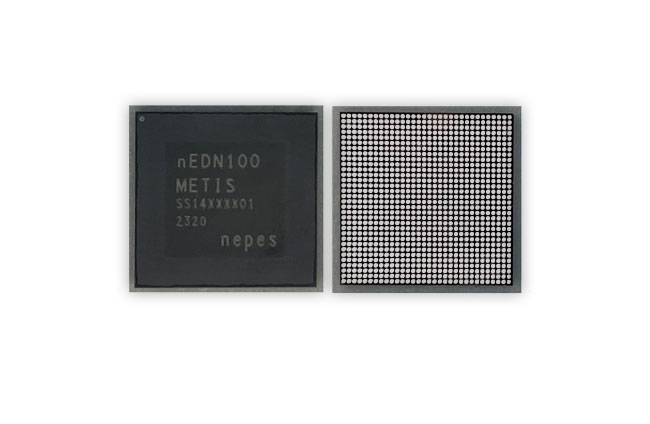 Nepes successfully develops ‘Metis’, an intelligent semiconductor for edge computing
-National project successfully completed... Optimization of manufacturing inspection equipment Deep learning acceleration IP development ▲Intelligent semiconductor ‘Metis’ for edge computing equipped with deep learning acceleration IPNepes (CEO Byeong-gu Lee), a cutting-edge semiconductor back-end process foundry company, announced on the 27th that it had succeeded in developing ‘METIS’, an intelligent semiconductor for edge computing.In April 2021, Nepes Artificial Intelligence Research Institute was selected as the 'Development of Intelligent Edge Computing Semiconductor for Lightening Manufacturing Inspection Equipment' project in the 'Artificial Intelligence Semiconductor Application Technology Development Project' hosted by the Institute for Information and Communication Planning and Evaluation (IITP) under the Ministry of Science and ICT in April 2021. was selected as the host company and conducted research through an industry-academia-research consortium with the Korea Institute of Electronic Technology and Hanyang University.The researchers developed a deep learning model for ultra-lightweight/ultra-precision manufacturing inspection equipment based on an automatic lightweight software framework with the research goal of ultra-lightweight/miniaturization, low-power consumption, and low-cost of existing server- or PC-based manufacturing inspection systems. Furthermore, using this, a deep learning acceleration IP optimized for data reuse and parallel computing processing was completed and installed on Metis.As a result, Nepes has developed a neural network-based deep learning defect detection algorithm that can reorganize the existing server-centered AI system into a terminal-centered one, and has secured a low-power SoC platform technology that reflects this. Through technological advancement, it has been able to increase productivity and efficiency at the manufacturing site. We hope to be able to contribute.In addition, Metis applied cx-BGA (Ball Grid Array) of nePACTM, Nepes' cutting-edge 2.5D & 3D package platform. nePACTM is a next-generation cutting-edge package technology that implements multi-layer and fine RDL wiring based on fan-out technology and flip chip bonding technology, and is suitable for highly integrated, high-performance chips such as artificial intelligence semiconductors.Yeonsook Park, head of Nepes Artificial Intelligence Research Center, said, “Through this research, we will solve network traffic issues in existing cloud server-type systems and secure intelligent processor technology that can detect defects at the edge, thereby developing various deep learning-related applications needed throughout the industry. “We have been able to accelerate it,” he said.Meanwhile, Nepes is carrying out national projects to develop core packaging technologies for system semiconductors and AI semiconductors, such as 'Development of chiplet heterogeneous integration ultra-high-performance artificial intelligence semiconductors' with a total project cost of KRW 44 billion hosted by the Ministry of Science and ICT, as well as AI semiconductors specialized for on-device. We are working to secure original technology.
2023-12-27 -
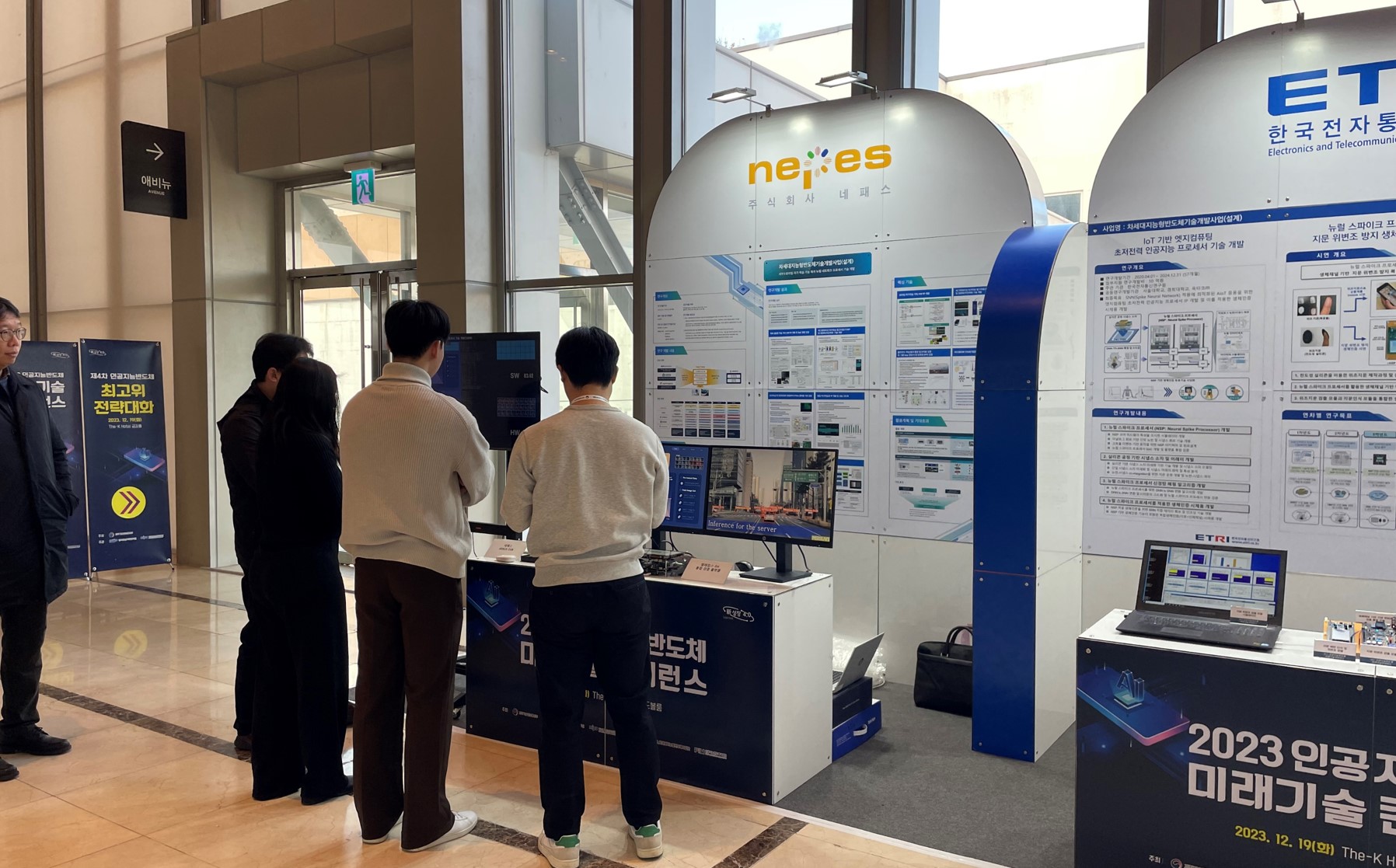 Nepes announces interim results of mobile self-learning processor national project
-Introducing artificial intelligence semiconductors equipped with self-learning NPU IP-Securing source technology to advance on-device AI semiconductor technology ▲ Nepes participated in the 2023 Artificial Intelligence Semiconductor Future Technology ConferenceNepes(CEO B.K. Lee), a cutting-edge semiconductor back-end process foundry company, presented interim results of the artificial intelligence (AI) semiconductor research and development national project at the ‘2023 Artificial Intelligence Semiconductor Future Technology Conference’ hosted by the Ministry of Science and ICT on the 19th This event is held every year, hosted by the Ministry of Science and ICT and organized by the Artificial Intelligence Semiconductor Forum, the Next-Generation Intelligent Semiconductor Business Group, and the Information and Communication Planning and Evaluation Institute to develop the AI semiconductor industry. In addition to exhibiting the AI semiconductor development achievements of participating companies, the Ministry of Science and ICT and domestic and foreign experts provide industry advice. We provide an opportunity to announce and discuss technology trends and major policy trends. At this event, which marks its 4th anniversary this year, Nepes exhibited 'JANUS', which has a mobile self-learning neural network processing unit (NPU) IP for object classification, and a distributed learning IP driving system. In particular, ‘Janus’ is a lightweight self-learning NPU IP-embedded artificial intelligence semiconductor developed to meet the needs of the market where the need for ‘on-device learning’ for optimal reconstruction (relearning) of artificial intelligence models in user development environments is emerging. This has a wide range of application fields, from intelligent automobile systems such as smart keys and driver monitoring systems through new user authentication to intelligent factory fields such as field learning systems to improve defect recognition rates.In April 2020, Nepes was selected as the lead organization for the ‘Development of mobile self-learning recursive neural network processor technology’ project in the ‘Next-generation intelligent semiconductor technology development project’ hosted by the Ministry of Science and ICT and is carrying out five years of research. This study aims to secure core technologies that enable lightweight semi-supervised learning and distributed learning by equipping devices with learning functions to optimize the privacy of personal and security data and the user environment. Many institutions, including Chungbuk National University, Hanyang University, and Seoul National University of Science and Technology, are collaborating. Based on its AI design technology, Nepes has not only secured on-device specialized AI semiconductor source technologies such as ‘mobile self-learning’ and ‘AI semiconductor lightweight’, but also developed on-device AI integrated platform technology. ▲ AI Chip with built-in lightweight self-learning NPU IP“The on-device AI semiconductor market is blooming, and in particular, AI semiconductors that can learn at the device level have endless applications in our daily lives,” said Park Yeon-sook, head of Nepes. “The result of this project is the development of on-device AI technology.” “It will secure fundamental technology for advancement,” she said. In addition, Nepes is developing its own cutting-edge technologies, such as 'Development of chiplet heterogeneous integration ultra-high-performance artificial intelligence semiconductor' with a total project cost of KRW 44 billion hosted by the Ministry of Science and ICT, and 'Development of core materials and process technology for 3D IC manufacturing using FOWLP' hosted by the Ministry of Trade, Industry and Energy. Based on packaging manufacturing technology, we are carrying out various national projects to develop core technologies for system semiconductor and AI semiconductor packaging.
2023-12-19 -
 Nepes' "Wafer Level Package" Selected as a 2023 World-Class Product
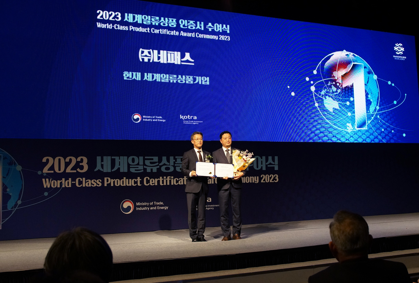
Advanced semiconductor packaging foundry specialist Nepes announced on the 9th at the 'World-Class Product Certification award Ceremony’ held at the Grand InterContinental Seoul Parnas, that their advanced packaging technology, Wafer Level Package (WLP), has been selected as a 'Current World-Class Product.'▲Nepes' WLP certified as '2023 Current World-Class Product' by the Ministry of Trade, Industry and Energy (Photo = Nepes) World-Class Products are distinguished annually by the Ministry of Trade, Industry and Energy and operated by the Korea Trade-Investment Promotion Agency (KOTRA), divided into 'Current World Class Products' and 'Next Generation World Class Products' to lead the global market, enhance corporate competitiveness, and contribute to export vitality. Nepes' Wafer Level Package was uniquely selected in the semiconductor sector as a 'Next Generation World Class Product' in 2016. Since then, it has renewed its certification, meeting conditions such as ranking within the top five in global market share and 5% or higher, along with an annual export scale of at least five million dollars, thereby newly elevating to the status of a 'Current World Class Product.' Wafer Level Packaging is an advanced packaging technology that performs bumping and Redistribution Layer (RDL) on fully processed wafers, differing from conventional packaging. Nepes successfully mass-produced advanced packaging applying bumping technology for the first time in Korea in 2000. Semiconductors utilizing this technology have significantly improved electrical characteristics due to shorter external connection wiring and also boast excellent heat dissipation properties, preventing overheating and effectively reducing production costs. Moreover, by forming solder bumps on the chip's I/O pads, replacing wires, it enables miniaturization and high integration, and is currently widely applied in mobile, PC, cameras, and more. Nepes has grown to become a core value chain in the domestic system semiconductor ecosystem based on commercializing advanced technologies such as Fan-out WLP and Fan-out Panel Level Package (FO-PLP), in a domestic market scarce of system semiconductor players. Currently, with global-level technology and manufacturing competitiveness, Nepes is attracting prominent overseas customers to Korea, expanding and sophisticating advanced foundry infrastructure. At the event, Lee Sang-min, manager of Nepes' management planning team, who received the certification, expressed, "It is very meaningful that Nepes' advanced packaging technology has been recognized for its excellence and marketability in the semiconductor industry and elevated to a 'Current World Class Product.' We will continue to strive to drive the ecosystem of system semiconductors in Korea and sustain our growth." Additionally, Nepes presented a successful case study in the medium-sized enterprise category at the ceremony.
2023-11-09 -
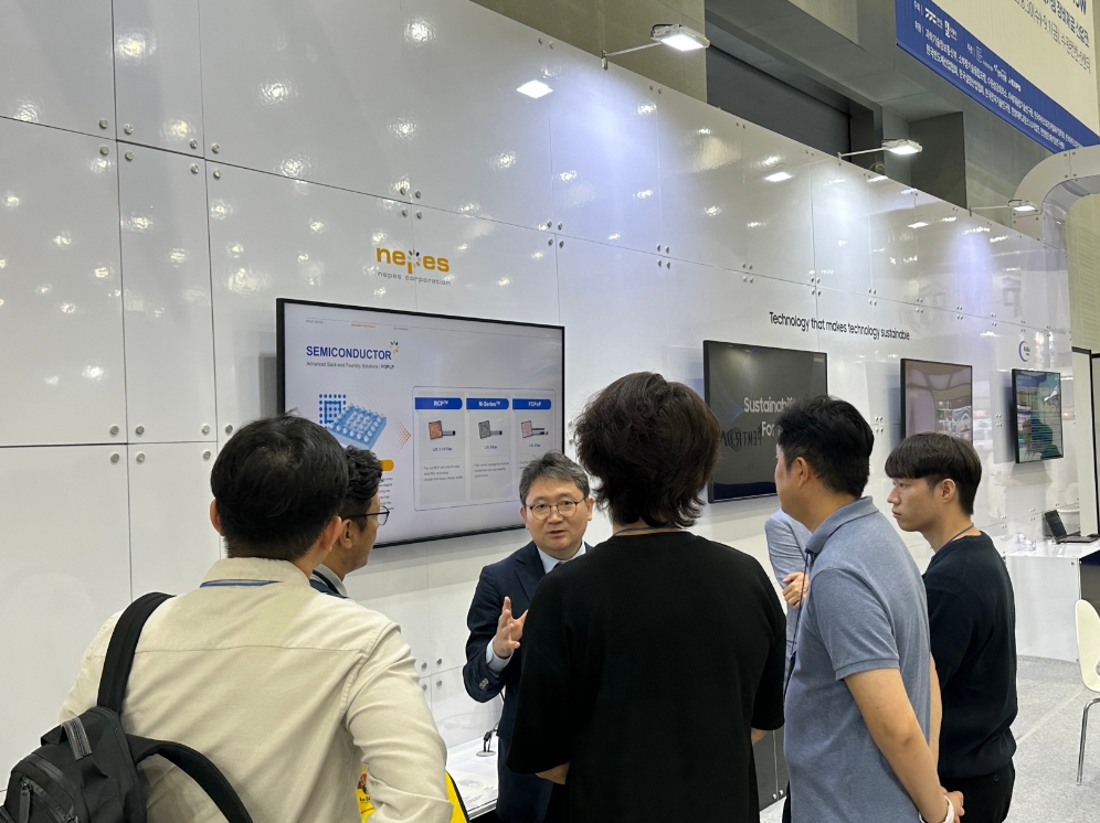
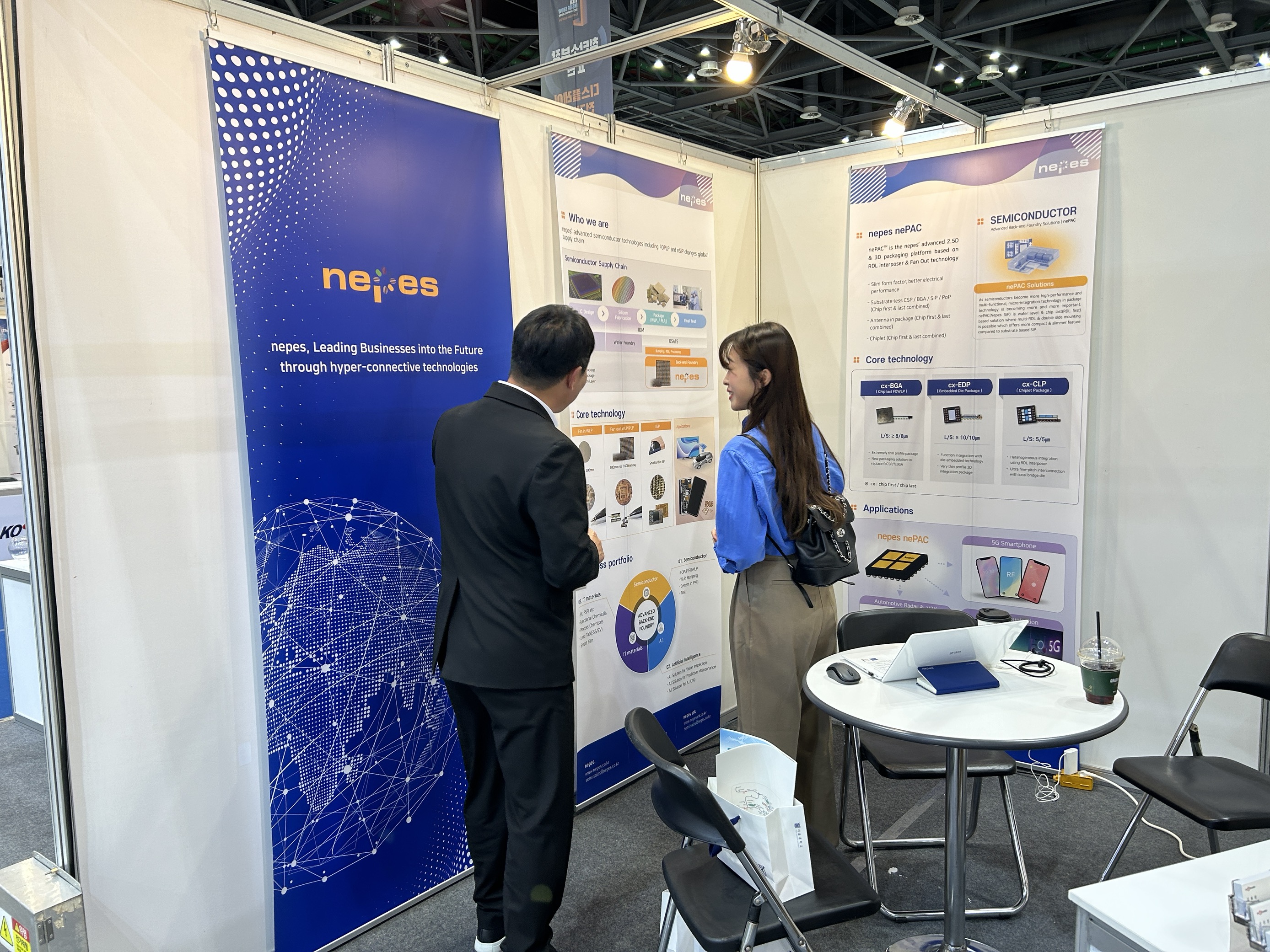 Nepes Captivates Attendees at '2023 TECH INSIDE SHOW' with Its nePAC Technology
The nePAC development team of Nepes participated in the [2023 TECH INSIDE SHOW], which took place from the 18th to the 20th at KINTEX. ▲An exhibit detailing the concept of nePAC (Photo = nePAC Product Technology Division) At the event, Nepes showcased their cutting-edge packaging platform, nePAC (nepes Package in Advanced CX solution), based on RDL interposer and Fan-Out technology. As their primary exhibition theme, the platform, which specializes in 2.5D & 3D packaging, garnered both intrigue and enthusiastic responses from industry professionals. ▲ A visitor at the Nepes booth listening to an explanation about nePAC. (Photo = nePAC Product Technology Division) Kim Hyo-Young, the team Leader in charge of the nePAC development team, who oversaw the participation in the exhibition, stated, "Visitors primarily asked many questions regarding the performance of nePAC technology and materials." He added, "This exhibition is the first for nePAC, and it provided a meaningful opportunity to broadly promote the technical expertise of Nepes."[The [2023 TECH INSIDE SHOW] is an event where South Korean companies, government entities, and organizations in the materials, components, equipment, and foundational industries participate. It serves to showcase the excellence of these industries in South Korea, promoting company products and technologies, and linking them to potential business opportunities.
2023-10-27 -
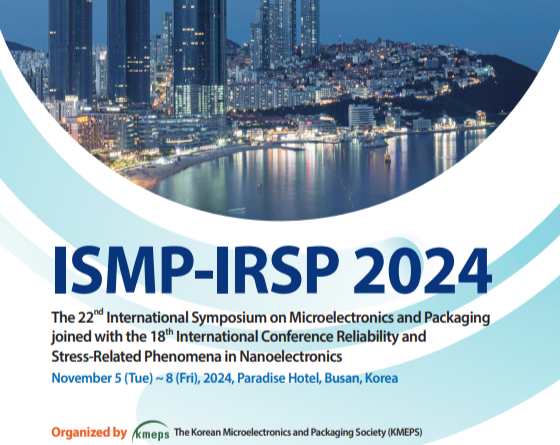
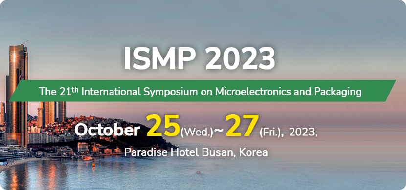 Nepes to Deliver a Lecture on "FO-RDL-Based 5G mmWave AiP Technology" at ISMP 2023
Nepes, represented by CEO Byung-Koo Lee, is set to participate in the International Symposium on Microelectronics and Packaging (ISMP) organized by the Korean Society for Microelectronics and Packaging (KMEPS) and deliver a lecture session. ISMP, now in its 21st edition, serves as a platform to explore the semiconductor packaging industry, share the latest technologies, and discuss strategies among various companies. Nepes, as the only domestic advanced packaging specialist, is returning to ISMP for the second time following its participation last year. In the "Package Design and Modeling2" session, Dr. Kang In-soo, the head of the semiconductor research institute, will present on the topic of "5G mmWave Antenna in Package based on Fan-out RDL Interposer Technology." The presentation will introduce Nepes' FO-AiP, highlighting its capabilities in reducing thickness and enhancing performance in antenna modules. The keynote speeches for the event will be delivered by Samsung Electronics and JCET. Additionally, attendees from 12 countries, including Korea, will explore the emerging trends in next-generation packaging technologies for industries such as artificial intelligence (AI), IoT, big data, and machine learning. ISMP 2023 will take place at the Paradise Hotel Busan from the 25th to the 27th of this month.[ISMP 2023 Home Page] ; https://www.ismp.or.kr/html/
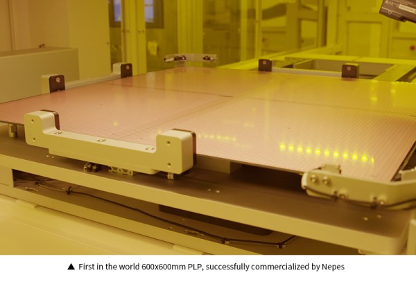
2023-10-23 -
 Nepes to Participate in 'SEDEX 2023,' Introducing Advanced Packaging Technology
Nepes, represented by CEO Byung-Koo Lee, will showcase its advanced packaging technology at the 25th Semiconductor Exhibition (SEDEX). SEDEX, celebrating its 25th anniversary this year, is the only specialized semiconductor exhibition in South Korea that encompasses all aspects of the semiconductor industry, including materials, components, and equipment. Nepes, along with industry leaders like SK Hynix and KEY FOUNDRY, will represent the semiconductor sector in Chungcheongbuk-do at the Chungbuk Joint Pavilion. At SEDEX 2023, Nepes plans to exhibit its core capabilities in advanced packaging technology, featuring 'nePACTM (Nepes Package in Advanced CX Solution)' and physical displays of 600mm FOPLP (Fan-Out Panel Level Packaging), as well as 300mm/200mm WLP (Wafer Level Packaging). They aim to introduce their advanced packaging technology, capable of reducing the thickness and enhancing the performance of semiconductors. SEDEX 2023 will feature the participation of around 250 domestic and international companies, including industry giants like Samsung Electronics and SK Hynix, occupying 800 booths. The event is scheduled to take place from the 25th to the 27th of this month at COEX in Samseong-dong, Seoul.[SEDEX 2023 Home page] ; https://sedex.org/public_html_eng/index.asp
2023-10-23 -
 Nepes commercializes advanced FO-PLP technology replacing PI material, featured in Japanese Electron
The "Electronics Device Industry News" of Japan published a visit report on Nepes on October 19, 2023. The highlight of the report, which featured an interview with Nepes CEO, Byung-Koo Lee, was the industry's first commercialized MDxTM(Molded Direct) technology in collaboration with Deca Technologies. This tech bypasses the use of Polyimide(PI), an essential material for the FO(Fan-out) technique, and only employs the Molding method to achieve FO-PLP. This simplification of the process is anticipated to serve as an alternative to the QFN(Quad Flat No-lead) process. Nepes plans to undergo testing until the end of 2023 and kick off mass production in 2024. They are especially looking to broaden the application of this technology in semiconductors for automobiles and expand their business into the Japanese market. In 2021, Nepes was recognized as one of the global TOP 10 advanced packaging companies in a semiconductor supply chain report released by the White House in the USA. They play a pivotal role in the advanced packaging sector. CEO Lee Byung-goo stated, "By building partnerships with major global semiconductor companies and continuously developing technologies that cannot be addressed with our current processes, our goal is to become a top-tier advanced packaging company globally within the next five years."
2023-10-19 -
 Nepes joins as a key partner for Samsung Electronics' Advanced Packaging (AVP) at the '2023 Advanced
Nepes, led by CEO Byung-Koo Lee, participated in the inaugural '2023 Advanced Semiconductor Packaging Show’ upon invitation from Samsung Electronics' AVP (Advanced PKG) business team. ▲ Kang In-soo, Executive Director, explaining Nepes' advanced packaging technology to the visitors. (Photo= Nepes) With the advanced semiconductor process facing significant costs and technical challenges, packaging technology to enhance chip performance is gaining attention. Last year, Samsung established an AVP (AdVanced Packaging) team to nurture advanced packaging and strengthen collaboration with technically capable partners. Having provided advanced packaging services since 2000, Nepes, as a core partner of Samsung, was invited to this exhibition, where they introduced their expertise through high-quality WLP processes, FOPLP, and the ultra-compact SiP, nePAC, captivating attendees' attention. Co-hosted by Suwon City and Gyeonggi Province, the '2023 Next-Generation Semiconductor Packaging Equipment and Materials Industry Exhibition', the first post-process specialized semiconductor exhibition in Korea, opened on the 30th and will run for three days at the Gyeonggi Suwon Convention Center, ending today(9/1).
2023-09-01 -
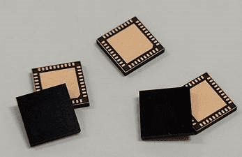 Nepes Laweh, World's First Commercialization of PI Alternative Packaging Technology
Leading advanced packaging company Nepes Laweh continues its innovation in advanced package technology, following the 600mm FOPLP (Fan-out Panel Level Package). Nepes Laweh announced that they have, for the first time in the world, implemented FOPLP solely through the Molding technique, without using the expensive Polyimide (PI), which is an essential material in the fan-out process.▲Implementation of FO-PLP using PI alternative packaging technology(Photo=Nepes) Based on Deca Technologies' M-Series™, this technology has been commercialized for the first time in the world by Nepes Laweh, and they have recently initiated product supplies to analog and automotive semiconductor company in the United States. This technology, which does not use PI, not only simplifies the process and improves productivity, but also has the potential to enhance product reliability. It is expected that this technology can extensively replace traditional conventional molding packages, such as QFN. In particular, analog semiconductor manufacturers, who frequently need to change and develop various products, can reduce the supply risk of materials like PCBs and lead frames. Additionally, it is a strong advantage that this technology allows for the transition to the fan-out process while maintaining existing semiconductor specifications, thus reducing the burden of new certifications for customers. Especially for products with large production volumes and stringent front-end customer certifications, such as automotive Microcontroller Units (MCU), the company expects this technology to offer advantages in manufacturing and quality control. A Nepes official conveyed, “The commercialization of fan-out molding technology is expected to further strengthen our technological competitiveness in the advanced package market.” Nepes Laweh has strategized to expand its customer base by applying fan-out PLP technology to various application products, including industrial and automotive products, starting with the supply of analog semiconductor samples.
2023-08-18
Investor Relations
NEPES, GLOBAL TOP-TIER PARTNER