

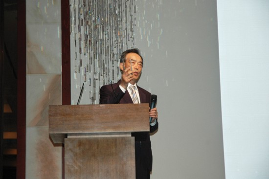
![[Report] Nepes, a Key Material, Part, and Equipment Company, Returns to Korea…Fitting Up the Supply 이미지1](https://www.nepes.co.kr/data/bbsData/17560882629.jpg)

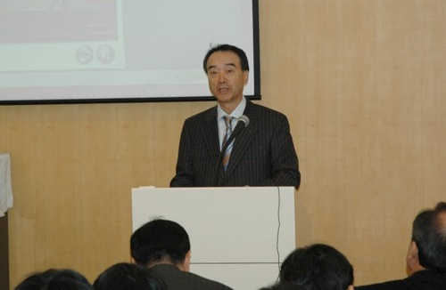
![[DIC2024] Nepes Increases Production and Reduces Costs for FO Packaging 이미지1](https://www.nepes.co.kr/data/bbsData/17461609729.jpg)

-
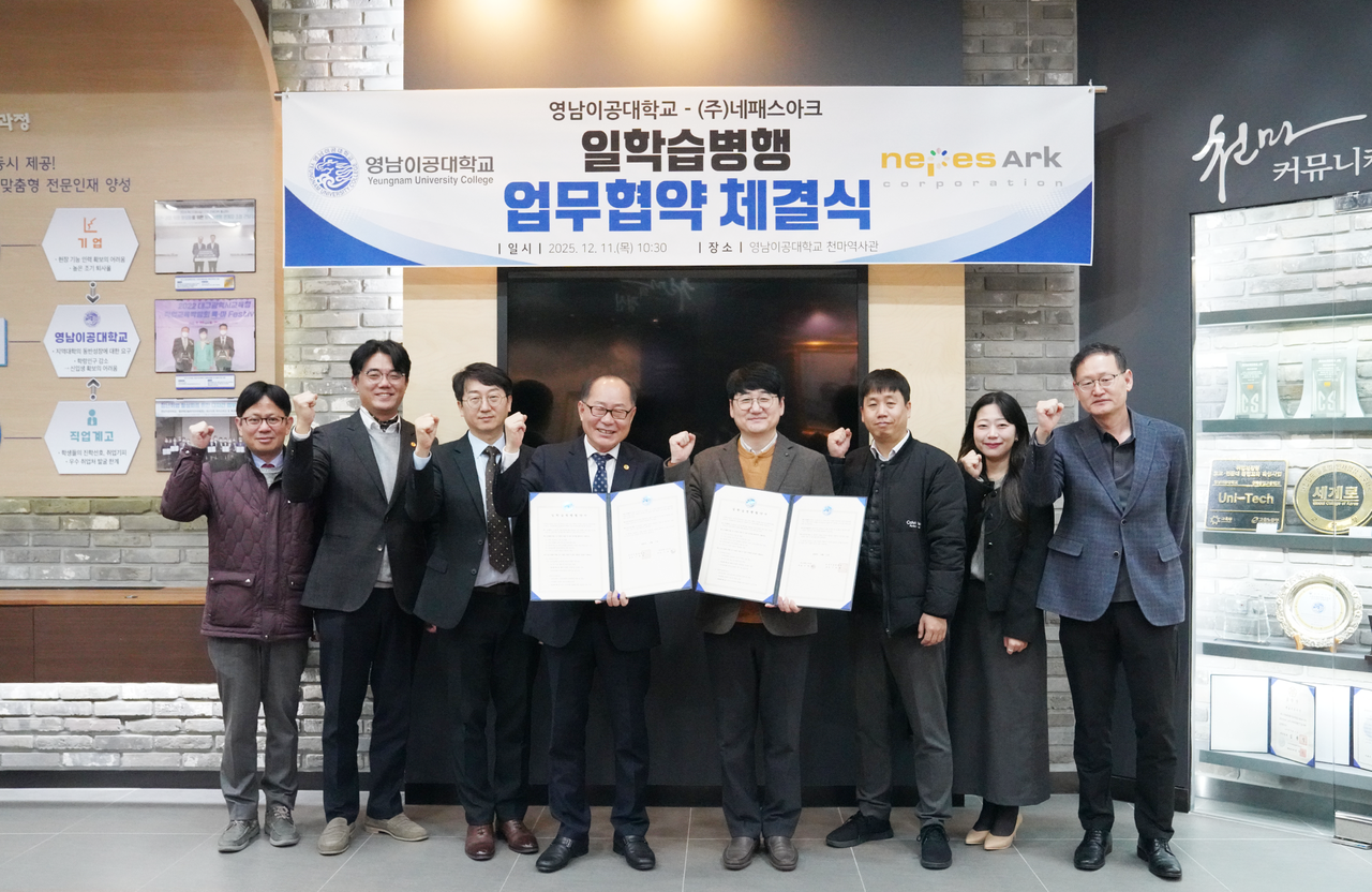
 NEWS
NEWS
-
 Nepes Laweh, World's First Commercialization of PI Alternative Packaging Technology
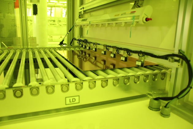
Leading advanced packaging company Nepes Laweh continues its innovation in advanced package technology, following the 600mm FOPLP (Fan-out Panel Level Package). Nepes Laweh announced that they have, for the first time in the world, implemented FOPLP solely through the Molding technique, without using the expensive Polyimide (PI), which is an essential material in the fan-out process.▲Implementation of FO-PLP using PI alternative packaging technology(Photo=Nepes) Based on Deca Technologies' M-Series™, this technology has been commercialized for the first time in the world by Nepes Laweh, and they have recently initiated product supplies to analog and automotive semiconductor company in the United States. This technology, which does not use PI, not only simplifies the process and improves productivity, but also has the potential to enhance product reliability. It is expected that this technology can extensively replace traditional conventional molding packages, such as QFN. In particular, analog semiconductor manufacturers, who frequently need to change and develop various products, can reduce the supply risk of materials like PCBs and lead frames. Additionally, it is a strong advantage that this technology allows for the transition to the fan-out process while maintaining existing semiconductor specifications, thus reducing the burden of new certifications for customers. Especially for products with large production volumes and stringent front-end customer certifications, such as automotive Microcontroller Units (MCU), the company expects this technology to offer advantages in manufacturing and quality control. A Nepes official conveyed, “The commercialization of fan-out molding technology is expected to further strengthen our technological competitiveness in the advanced package market.” Nepes Laweh has strategized to expand its customer base by applying fan-out PLP technology to various application products, including industrial and automotive products, starting with the supply of analog semiconductor samples.
2023-08-18 -
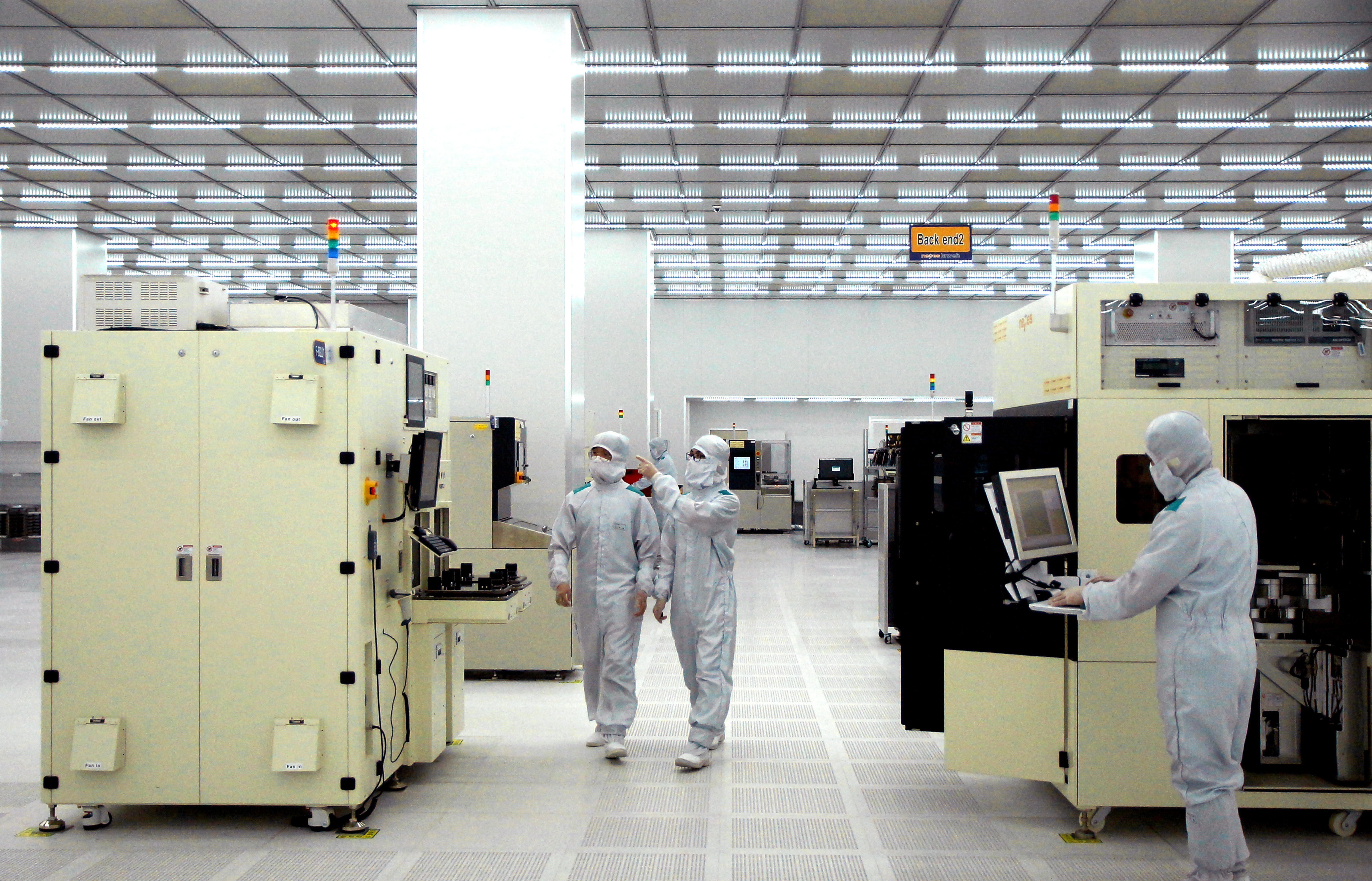
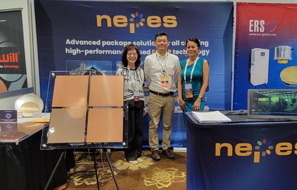 Nepes participated in the '2023 ECTC(Electronic Components and Technology Conference)'
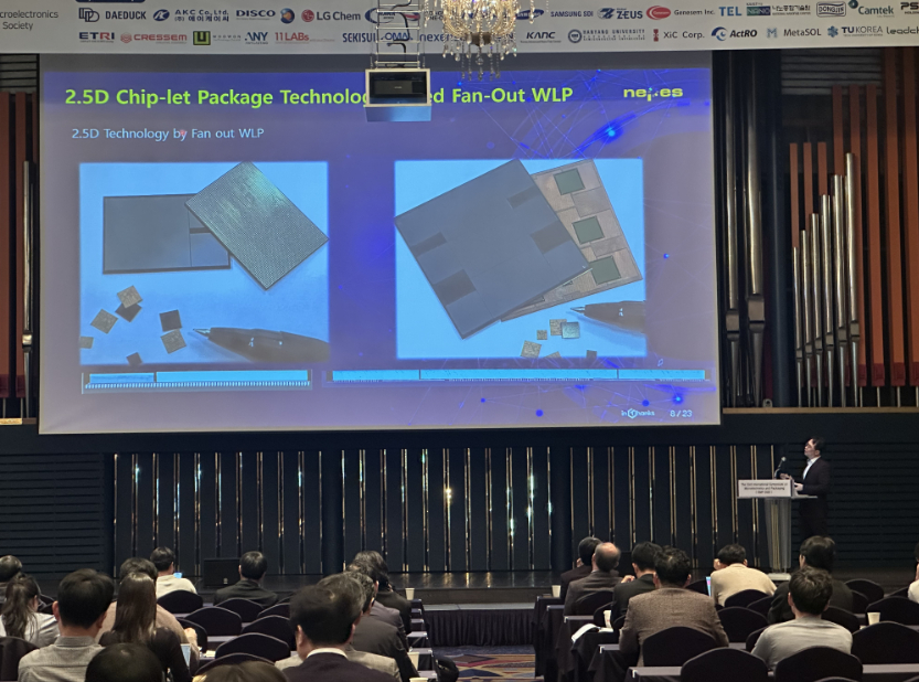
Nepes participated in the 2023 ECTC (Electronic Components and Technology Conference) held in Orlando, Florida, USA from May 30th to June 2nd and introduced its advanced semiconductor packaging technology. Celebrating its 73rd anniversary this year, ECTC is an international event hosted by the Electronics Packaging Society under the IEEE, and is a place where experts in the field of electronic parts, materials, packaging, and IoT attend to discuss next-generation semiconductor technologies. At this event, Nepes introduced next-generation PoP (Package on Package), 2.5D, and 3D stacking technologies as well as the world's first 600mm FOPLP solution that was successfully mass-produced. FOPLP is a next-generation packaging solution that implements a fan-out package on a large square panel with a size of 600mm × 600mm, a step forward from the existing 300mm circular fan-out wafer level packaging (FOWLP). On the 31st, a paper titled “6-Sided Die Protection for Chiplet Package with Multi-Layer RDL” was selected and presented.
2023-06-02 -
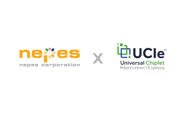 Nepes joins 'UCIe' consortium to establish semiconductor packaging standards
Nepes participate in the UCIe(Universal Chiplet Interconnect Express) consortium launched to establish an industry standard for ‘Next-generation chip packaging technology’.Semiconductor companies such as ▲AMD ▲Arm ▲Qualcomm ▲ASE, including TSMC and Intel, and IT companies such as ▲Google Cloud ▲Meta ▲Microsoft also participated in the consortium.The consortium aims to establish UCIe as a new connectivity standard such as PCIe, USB, NVMe, etc.Members will soon begin working on the creation of the next-generation UCIe technology standard, including the chiplet form factor, management, enhanced security and other essential protocol definitions after the UCIe 1.0 specification is drafted.If the UCIe standard is established, it is compatible with other companies' chiplet structures. This can lead to cost savings and faster time to market.
2022-08-19 -
 Nepes integrates packaging with advanced fan-out technology
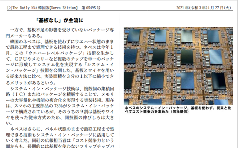
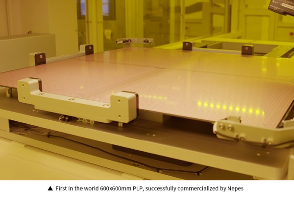
“Heterogeneous integration,” a hot keyword in the global semiconductor marketNepes’s fan-out technology-applied “nSiP” & “nPoP” are the alternativesThe global semiconductor industry started to focus on the back-end process. As Moore’s law, which states that the semiconductor density doubles every two years, is no longer valid, and miniaturization of circuits in the front-end process is reaching its limit, the industry players are looking for alternatives. Among the alternatives, the “Heterogeneous Integration Packaging,” also referred to as a 2D and 3D packaging has been gaining attentions as the next-generation technology. It attaches chips in series and integrates them to a single semiconductor piece. On July 7th,Nepes introduced its unique technology “nSiP’ and “nPoP” along with the trends of the next-generation heterogeneous integration packaging at “Semiconductor Packaging Day 2022” held by Electronics Times, a Korean IT news media.Nepes is an advanced semiconductor packaging company that supplies the Wafer Level Packaging(WLP), Fan-Out Panel Level Packaging(FOPLP) and more.It is a pioneer in the back-end process as it commercialized the FOPLP technology for 600x600mm square panels, not round panels, for the first time in the world in May 2017.System in Package(SiP) introduced by Nepes at the conference, is a heterogeneous integration packaging technology with various functions put into a single chip. Nepes’s unique technology “nSiP” does not contain components such as substrates, reducing the packaging size to one third and shortening the signal transmission distance by 30% for performance improvement. Nepes produced its first commercialized nSiP in January. Package on Package(PoP) is a technology that adds a layer of package with a different function on top of another package. This technology minimizes heat generation from the chips and lowers the packaging thickness by 26% compared to competitors’ products. Mass production is scheduled to be in 4Q, 2023.Nepes’s unique packaging technologies are based on the Fan-Out technology that utilizes the Re-Distribution Layer(RDL). In the Fan-Out technology, the input/output terminals are located outside the chips to fit in a higher number of terminals. It is expected to be the solution for the ultra-high-performance and high-integration packaging market since it can be used to layer or expand different sizes of chips as well as to improve the electrical properties and thermal efficiency, In the meantime, the global packaging market size is expected to be driven by the SiP, Fan-Out, and PoP technologies and reach a $9.6 billion scale by 2026 according Yole, a market analysis firm. The PoP’s market share is expected to increase particularly high from 5% to 11%. Read more: https://www.digitaljournal.com/pr/nepes-integrates-packaging-with-advanced-fan-out-technology#ixzz7aC8RY0hV
2022-07-27 -
![[Semiconductor Packaging Day 2022] Nepes expands the application area of FO-PLP. - ETnews 썸네일](https://www.nepes.co.kr/data/bbsData/16576096149.jpeg) [Semiconductor Packaging Day 2022] Nepes expands the application area of FO-PLP. - ETnews
[Semiconductor Packaging Day 2022] Nepes expands the application area of FO-PLP. - ETnews[Semiconductor Packaging Day 2022] Nepes expands the application area of FO-PLP. Nepes will expand its mass-production products using fan-out-panel level packages (FO-PLP), one of the most advanced packaging technologies. Following the Power Management Integrated Circuit (PMIC), market will be expanded with codec chips and application processors (AP). It will also respond to demand for next-generation packing markets such as system-inpackage (SiP) and 2.5 and 3D utilizes Nepes' advanced fan-out (FO) technology. During the “Semiconductor Packaging Day 2022”, Kim Jong-heon, Nepes' Corporate CTO of Semiconductor Business (Executive Vice President), said in “We are increasing applications such as codecs after last year’s mass-production of the world’s first PMIC with FO-PLP", “We will mass-produce AP, and APU, which combines AP and GPU, as FO-PLP in the future.,” he addedFO-PLP is a technique that packages square panels rather than round warfers. Nepes has a mass production technology of 600mm panels in width and height. It is considered a next-generation technology that can increase production speed by more than five times compared to packaging on a typical 12-inch wafer. Nepes have been supplying PMIC of global semiconductor companies with FO-PLP since the fourth quarter of last year. For the first time in the industry, Nepes has invested hundreds of billions won in building FO-PLP mass production facilities. Nepes have also begun the mass production of codec chips as well as PMIC. It is known that other chips, such as AP, are currently being discussed with customers for the mass production of FO-PLP. The specific customer company is not disclosed. Vice President Kim said, “In addition to single-chip FO-PLP, there are many more products when considering the packaging of two or more chips. The expansion of the FO-PLP market is as expected. Nepes will also be launching its next-generation packaging market. Typical examples are 2.5D and 3D packaging, and 3D package-on-package (PoP) technology. PoP is a technology that stacked packages which function differently from packages. Nepes developed an ultra-thin PoP with minimal heat and reduced package thickness and passed the technical qualification. Vice President Kim explained that the packaging thickness can be reduced up to 26% compared to his competitors. SiP without substrates is also a field that Nepes focuses on. It introduced its first mass-production product earlier this year with SiP that utilizes Nepes' own RDL technologies. It reduces the size to one-third of the existing package and shortens the signal transmission distance by 30%. Nepes is also developing a 3D stacking technology that vertically stacked semiconductors. Nepes' entry into the next-generation packaging market is based on its excellent fan-out technology. Fan-out is a technology that increases the number of I/Os by placing semiconductor input and output terminals (I/O) outside of the chip and can exchange more signals. Vice President Kim said, “Nepes possesses a wide range of advanced packaging technologies to provide packaging solutions that are ahead of their time.”he also said “We plan to play a role as a high-tech back-end foundry rather than a simple back-end process.”
2022-07-12 -
 Nepes joins the American Semiconductor Innovation Coalition (ASIC)
Nepes joins the American Semiconductor Innovation Coalition (ASIC) to Strengthen Global Semiconductor CooperationNepes, led by Chairman Lee Byung-Koo, has announced its participation in the American Semiconductor Innovation Coalition (ASIC) to help strengthen global semiconductor cooperation. As members of ASIC, Nepes will contribute to developing a strong proposal for a technical agenda in advanced packaging. ASIC is a coalition of more than 75 businesses, startups, universities, national labs, and nonprofits dedicated to bringing the best research and development to the National Semiconductor Technology Center (NSTC) and the National Advanced Packaging Manufacturing Program (NAPMP). It aims to strengthen the diverse and competitive semiconductor workforce, make bold investments in semiconductor R&D, and academic infrastructure needed to deliver semiconductor innovation, prototyping and manufacturing in the United States. Dr. Douglas Grose, who is leading ASIC, said, “ASIC is focused on working collaboratively to develop new strategies and solutions for the U.S. semiconductor industry, and that includes partnerships with international organizations. We’re very pleased to have Nepes join ASIC and provide their expertise on advanced packaging, which is increasingly critical to the semiconductor industry both in the U.S. and worldwide.” ASIC member companies include key companies in the semiconductor field in Korea, the US, Europe, and Japan. As OSAT companies, i3 Microsystems of the US and Nepes of Korea are participating.“As the importance and role of advanced packaging technology continues to grow, ASIC enables Nepes to further strengthen cooperation with leading global member companies,” said Kim Tae-hoon, president at Nepes. “It has given us an opportunity to raise the status of Korean companies’ advanced packaging technology and contribute to the development of the advanced back-end industry and the global semiconductor ecosystem.”
2022-06-21 -
 Nepes promotes new packaging technology at an international conference
Nepes promotes new packaging technology at an international conferenceThe packaging provider introduces ‘nPLP’, a next-generation packaging solution The company also presents FOWLP-based antenna-in-package technology on the 3rd of this month Nepes presented at the 2022 Electronic Components and Technology Conference (ECTC), which took place in San Diego from May 31 to June 3 (PDT), to showcase its cutting-edge semiconductor packaging technology.Organized by IEEE Electronics Packaging Society, the conference is an international event attended by experts in the fields of electronic components and materials, packaging, and IoT to share their visions about future technology and discuss methods of cooperation. This year marks the 72nd iteration of ECTC. The 2022 ECTC brings together 106 corporations from 24 countries, including Nepes, Samsung Electronics, TSMC, and Amkor Technology. This year, Nepes became the world’s first company to successfully mass-produce its nPLP solution. An improvement over the previous 300-mm round FOWLP, nPLP is a next-generation packaging solution in which a fan-out package is implemented onto a 600-by-600-mm large-size square panel. Lewis Kang, the Managing Director of the Future Technology Planning Division gave a talk titled “FOWLP-based antenna in package (FO-AiP) using 5G mmWave) on June 3, the last day of the event. Kang introduced the antenna-in-package technology, which can reduce signal loss in 5G smartphone communication antennae using Nepes’ noteworthy fan-out technology. “We promoted Nepes’ unique PLP and AiP technology for 5G use at the international ECTC conference, which is attended by semiconductor experts from all over the world alongside possible clients,” said Kang. “We paved the way for future discussions regarding new business developments with possible global, top-tier clientele attending the conference.”
2022-06-14 -
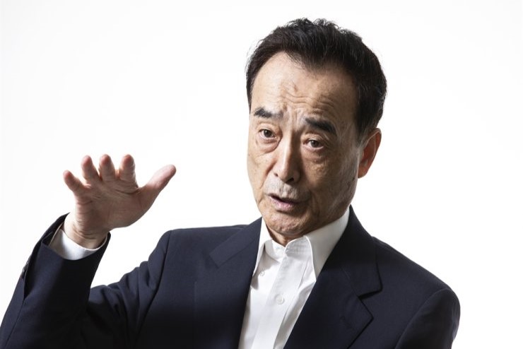
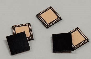
 Nepes, which eliminated semiconductor leadframe, “semiconductor packaging efficiency 10 times… Achie
Nepes, which eliminated semiconductor leadframe, “semiconductor packaging efficiency 10 times… Achieved 1 trillion won in sales within 3 years”Semiconductor manufacturing is divided into a ‘pre-process’, in which a circuit is engraved on thin silicon to manufacture a chip, and a ‘post-process’, in which the manufactured chip is packaged (packaging) using a substrate and metal wire. Nepes a company specializing in semiconductor backend-processing, recently started produce the 'Fan-out panel level packaing'(FOPLP) that packaged high-performance semiconductors with a thickness of 0.9nm and works in the form of a square panel(600mm) It is the only technology in the world that increases the net die (the number of chips per wafer or panel) more than tenfold from 1,000 to 10,000. Since there is no wasted area on the edge of the circular wafer, productivity is also greatly improved. Lee Byung-koo (pictured), chairman of Nepes, said, “We are pushing the semiconductor packaging technology to the limit through FOPLP and others." Nepes, a listed company on the KOSDAQ, is a cutting-edge company in the packaging field. They mainly receive chips from Samsung Electronics, etc., and package them to complete semiconductors. It has the capacity to process 1104,000 wafers per year. Sales are 65% export and 35% domastic. Last year, it recorded 418.4 billion won in sales and 16.4 billion won in operating loss. Nepes has been developing a technology for packaging chips to be light, thin and short (light, thin, short and small) so that semiconductors can be put into smartphones and IoTs. In the past, semiconductors were shaped like a black centipede. Its size was much larger than the chip. This is because the chip was placed on the board, a connection part similar to a centipede was made using a copper wire, etc., and then an epoxy resin was placed on it to fix it. Due to its complex structure, the heat problem was also serious. In contrast, the semiconductors packaged by Nepes do not change significantly in the size of a square chip. This is because they developed 'Wafer Level Packaging (WLP)' technology in the 2000s, which coats a thin metal film just below the chip, prints a circuit diagram with a laser, and sends and receives electrical signals using fine metal protrusions. The thickness of the finished semiconductor was only 0.4 nm. Overseas semiconductor manufacturers that have recognized Nepes' technology have sent their chips by air to request packaging. Nepes, which eliminated semiconductor centipedes, “semiconductor packaging efficiency 10 times… Achieved 1 trillion won in sales within 3 years” Nepes spares no expense in R&D and facility investment to maintain cutting-edge technology. Last year, an additional 42,962㎡ factory site was prepared in Goesan, North Chungcheong Province, and advanced packaging facilities such as WLP and FOPLP were installed. Last year's operating loss is related to such facility investment. Nepes' earnings are expected to improve significantly this year. This is because the total production capacity will increase by about 60% when the FOPLP facility starts operation. The securities industry predicts that Nepes will record 606 billion won in sales and 52 billion won in operating profit this year. This is almost twice as much sales as in 2020 (343.6 billion won).
2022-05-09 -
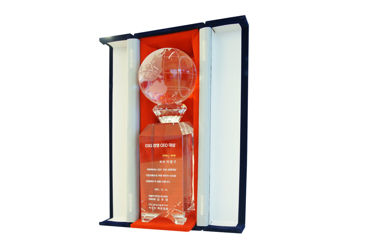 Nepes wins the ESG Management CEO Grand Prize
Nepes won the ESG Management CEO Grand Prize (Corporate Governance Sector) at the ‘2021 ESG Management Awards Ceremony and Best Case Presentation’ held at the National Assembly Hall conference room on December 15th.This event was co-hosted by the Office of National Assembly member Joo-Young Kim and the Audit and Sharing Research Institute, and was prepared to further vitalize and encourage ESG management, which is indispensable in corporate activities.The organizer selected the ESG management target awardees based on the company's sustainability report, and included 9 environmental indicators such as general energy consumption, renewable energy consumption, and greenhouse gas emissions, and 12 other environmental indicators including employee safety, win-win growth support for business partners, and support for local communities. Each of the nine governance indicators, such as social indicators, management performance evaluation and compensation, identification of stakeholder ESG needs, and participation in global partnerships, was scored and evaluated. Nepes Chairman Lee Byung-koo was selected as the best CEO in the corporate governance sector and received this award.
2021-12-22 -
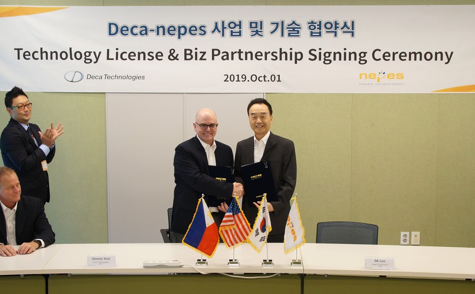
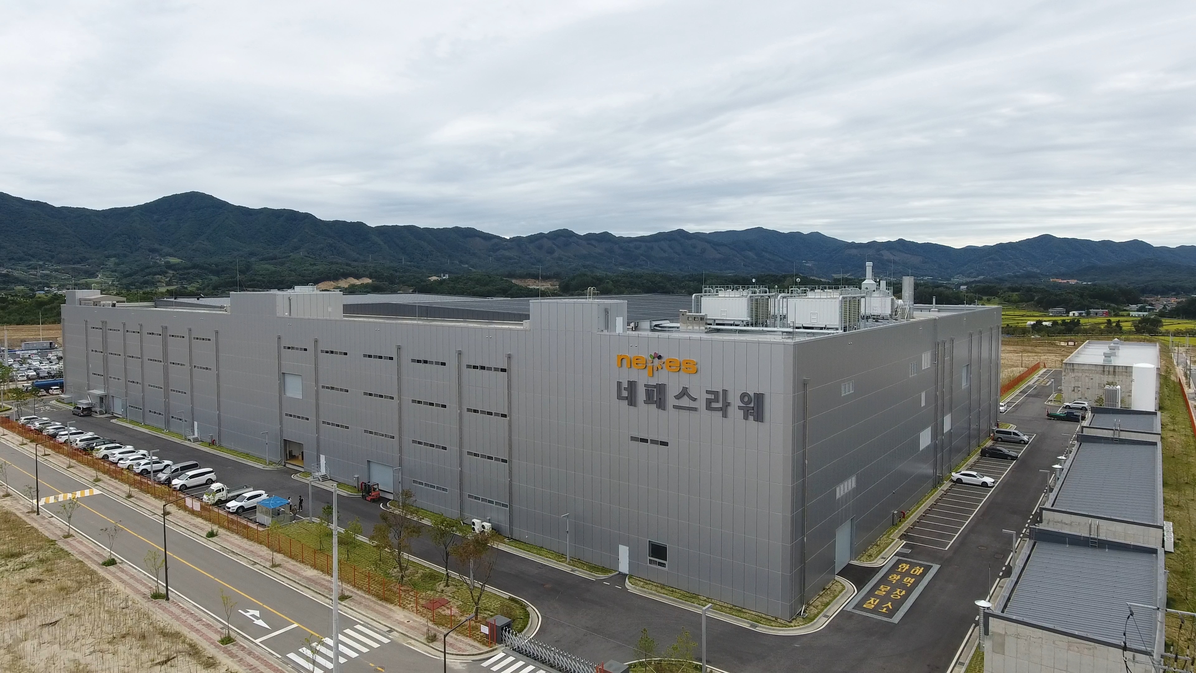 Nepes Laweh set new industry benchmark with 600mm large panel M-Series fan-out volume production
Nepes Laweh corporation announced the successful production qualification and ramp-up of the world’s first 600mm x 600mm large panel manufacturing line using Deca’s M-Series™ fan-out technologies. Nepes Laweh held the completion ceremony of the Cheongan Campus PLP Line on December 7th with the presence of Minister of Trade, Industry and Energy, Governor of Chungcheongbuk-do, and representatives of customers and partners. The company announced that the FOPLP line completed customer certification in the third quarter and secured a stable yield and entered full-scale mass production. The PLP fab, which held the completion ceremony this time, was the first fab built on the 186,000㎡ Cheongan Campus site with 25 soccer fields, and was a total building area of 34,000㎡. This is a level that can produce up to 96,000 panels per year based on 600mm PLP. Based on this next-generation manufacturing line, Nepes is evaluated to be able to provide high-density packaging solutions required for advanced system semiconductors for each application, such as smartphones, automobiles, and IoT, according to customer needs. "FOPLP is the best packaging solution for high-end semiconductors as a result of long cooperation with global partners such as materials, parts, and equipment," said Chilhee Chung, Chairman of Nepes and GM of Semiconductor Business “We’re pleased to be working with nepes to bring the industry’s largest format 600mm square panel to volume production” commented Tim Olson, CEO of Deca. “With initial production focused on single and multi-die packages for leading Smartphone producers, the future is heterogenous integration of chiplets using Deca’s Gen 2 technology. A recent customer application with 10 embedded chiplets was designed into a 36mm x 36mm package. Such a large device is limited to 73% maximum utilization on 300mm round format due to edge losses. On 600mm, the utilization jumps to 92% delivering greater than 25% cost reduction on area utilization alone.” About Nepes Laweh www.nepes.co.kr Nepes Laweh is leading company in the system semiconductor industry with advanced fan-out packaging solution. In the era of the 4th industrial revolution, when semiconductors are refined and advanced, such as 5G, self-driving cars, and smartphones, we are presenting new standards for fan-out packages based on nPLP™ technology using 600mm large square panels. About Deca Technologies www.ThinkDeca.com Deca is a leading provider of advanced packaging technology to the semiconductor industry with M-Series™ fan-out and Adaptive Patterning® real-time design-during-manufacturing. A growing list of industry leaders have completed technology transfer and license agreements for access to Deca’s proven structures, processes, materials, equipment, design systems and know-how. Starting with the highest quality and reliability in Gen 1 aimed at Smartphone applications to the growth of Gen 2 for chiplets and heterogeneous integration, Deca’s technologies are emerging as key industry standards for the future.
2021-12-09 -
 Nepes Laweh started Volume Production of ‘FOPLP’, a next-generation packaging solution
- Stable yield achievement of 600mm FOPLP Fab at Cheongan Campus ... Mass production ramp-up - The world's first large-panel packaging process enabling significant productivity improvement and more accessibility to 'advanced technology' Nepes Laweh announced that it will more than double its capacity next year as it begins mass production of FOPLP, the next-generation packaging process. Nepes Laweh held the completion ceremony of the Cheongan Campus PLP fab on December 7th with the presence of Minister of Trade, Industry and Energy, Governor of Chungcheongbuk-do, and representatives from customers and partners. The company announced that the FOPLP manufacture line completed customer certification in the third quarter and achieved a stable yield and started full-scale mass production and plans to more than double its capacity next year aligned with strong customer demand. The PLP Fab, where the completion ceremony was held, was the first fab built on the 186,000㎡ Cheongan Campus site which is the size of 25 soccer fields: with a total building area of 34,000㎡. The fab can produce up to 96,000 panels per year based on 600mm PLP. Based on this next-generation packaging line, nepes would receive a favorable evaluation about her ability to provide high-density packaging solutions required for Non-memory semiconductors for each application, such as smartphones, automobiles, and IoT, aligned with customer needs. "FOPLP is the best packaging solution for high-end semiconductors as a result of long cooperation with global partners such as materials, parts, and equipment," said Chilhee Chung, Chairman of Nepes and GM of Semiconductor Business According to the industry, nepes laweh's FOPLP is a large square panel with a size of 600mm by 600mm, and it is analyzed that productivity has greatly improved compared to the 300mm round FOWLP. In particular, the fan-out technology applied to Nepes Laweh’s FOPLP has been proven to have high stability compared to existing technologies. As demand increases mainly from advanced semiconductor manufacturers in the future, its market share is expected to significantly increase in the overall packaging market. About Nepes Laweh Nepes Laweh is leading company in the system semiconductor industry with advanced fan-out packaging solution. In the era of the 4th industrial revolution, when semiconductors are refined and advanced, such as 5G, self-driving cars, and smartphones, we are presenting new standards for fan-out packages based on nPLP™ technology using 600mm large square panels.
2021-12-07
Investor Relations
NEPES, GLOBAL TOP-TIER PARTNER